
Wakahara, Akihiro
| Affiliation | Institute for Community Innovation in collaboration with KOSEN |
|---|---|
| Title | Professor |
| Fields of Research | Semiconductor Physics / Optoelectronics / Crystal Growth |
| Degree | Dr. of Engineering (Toyohashi University of Technology) |
| Academic Societies | Japan Society of Applied Physics / Institute of Electronics, Information and Communication Engineering / Japanese Association for Crystal Growth / MRS Japan |
| wakahara@ Please append "tut.jp" to the end of the address above. |
|
| Laboratory website URL | http://www.int.ee.tut.ac.jp/oeg |
| Researcher information URL(researchmap) | Researcher information |
Research
Recent demand of highly advanced information processing requires much faster processing system. But the performance of time sequential series information systems composed of a conventional electronic device are going to reach the limitation. On the other hand, it is expected that a photoelectronic-integrated-system takes an important role in a future information processing system, because a parallel processing system using optical system has high performance in image processing.
In this laboratory, we focus on following two big issues to realize a fusion of photonic and electronic devices.
(1)R & D of heteroepitaxy of high quality semiconductor which has high luminescence capability on Si
(2)R & D of new photoelectronic integrated processing system by utilizing the parallel communication nature of the information that light has.
In order to overcome these subjects, we are aiming at the solution of problems produced due to the integration of compound semiconductor based photonics and Si-based electronic systems by investigating wide range research field from crystal growth to elucidation of fundamental properties of materials and device.
In addition, we are exploring a frontier of high functional devices, which would be created by technology fusion of these novel technology for photoelectronic integration and highly developed Si-technology including LSIs and/or MEMS. These research projects are carried out at unique research centers, Electron Device Research Center and Venture Business Laboratory, in which both compound semiconductor based device and Si CMOS can be processed simultaneously.
Theme1:Reserch of monolithic integration of phtonic and electronic devices
Overview
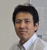
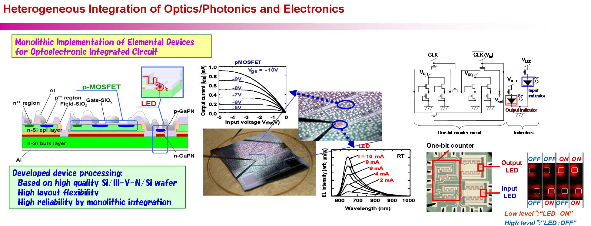 Figure 1 . Concept of monolithic integrated photo-electronic system and a test-chip micrograph.
Si LSI technology is facing big wall of the size and/or thermal budget.
We have been investigating an optoelectronic parallel processing chip by integrating photonics and electronics.
We proposed the seamless fabrication processing of photonic and electronic devices by using Si/III-V/Si wafer.
As an example, we succeeded to grow a structural defect-free Si/III-V-N/Si heterostructure by the elucidation of the crystal growth mechanism at the atomic level, and demonstrated a digital circuit with optical output by using this heterojunction wafer.
Keywords
Theme2:Heterogeneous integration of III-Nitrides and Si devices
Overview
 Monolithic OEIC fabricated in Si/SiO2/GaN wafer
GaN-based devices have an excellent heat resistance and chemical resistance, and thus it has a potential for implementation into a Si CMOS LSIs by using Si wafer embedded III-N device structure.
In this project, we have been developing a devices composed of GaN-based photonic devices, such as micro-LED and/or UV-photodiode arrays, and Si circuit.
These devices are fabricated by using III-Nitiride processing line installed in EIIRIS.
Keywords
Title of class
Undergraduate: Fundamental Electrical Circuitry, Analytical Electromagnetism 1, Solid State Electronics 1 /
Graduate: Electronic Devices, Advanced Microelectronics 2, R & D management for Interdisciplinary Research, Advanced GI Management 1 & 2