
ここからコンテンツです。
A higher level of sensitivity and smaller size for diamond magnetic sensors
Next-generation diamond quantum sensors using nanostructures Ryota Katsumi
A research team led by Assistant Professor Ryota Katsumi and Professor Takashi Yatsui from Toyohashi University of Technology’s Department of Electrical and Electronic Information Engineering along with Professor Masaki Sekino from the University of Tokyo’s School of Engineering has shown that a structural design using nanostructures can further enhance the sensitivity of diamond quantum sensors. The results of this research were published in the Japanese Journal of Applied Physics (JJAP) on July 3, 2022.
Nitrogen-vacancy (NV) centers are point defects that form in diamond and have outstanding optical and spin properties. Therefore, it is theoretically understood that if collective NV centers in diamond are used as quantum sensors, it may be possible to achieve high-sensitivity magnetic detection at room temperature. This approach is garnering considerable attention as a potential next-generation, high-performance magnetic sensor. However, reported problems with quantum sensors based on NV centers are that they have a lower level of sensitivity than existing sensors, such as superconducting quantum interferometers. If it is possible to improve the luminescence detection efficiency from NV centers, the magnetic sensitivity can be improved, but due to diamond fabrication being technically difficult, no design has been made to improve the luminescence extraction efficiency of the collective NV center.
In this research, we proposed a resonator device structure that enables enhancement of the luminescence intensity of the NV center and highly efficient luminescence extraction, as shown in the figure, with the aim of achieving a diamond quantum sensor capable of highly sensitive magnetic detection. Using the same structure allows for the further enhancement of the magnetic sensitivity of the NV center, which is expected to be dozens of fT/√Hz. This is equivalent to existing sensors, such as superconducting quantum interferometers. Furthermore, the device size is small, at only a few µm, allowing for a significant reduction in the required optical power.
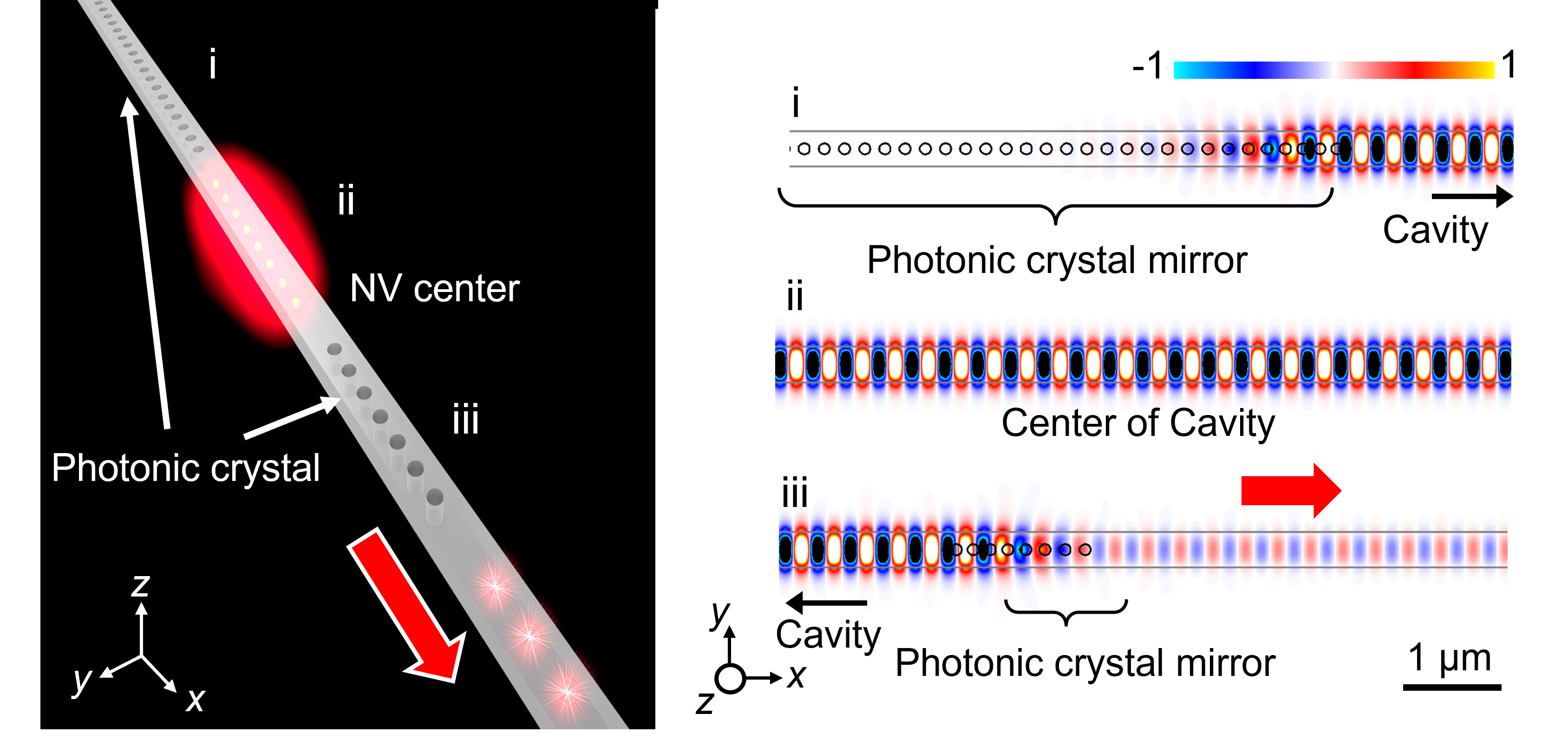
Device structure (left) and Calculation results of electromagnetic field simulation (right).
The research team believes that this design device can be produced using existing diamond fabrication techniques. Ultimately, the research team believes that this design can be combined with other integration and optical communication technologies to create the next generation of practical quantum sensors.
The results of this research have been published in the Japanese Journal of Applied Physics (JJAP) on July 3, 2022, an English-language journal published by the Japan Society of Applied Physics.
This research is supported by the Quantum Leap Flagship Program (Q-LEAP, JPMXS0118067395) of the Ministry of Education, Culture, Sports, Science and Technology of Japan. It is also supported by Grants-in-Aid for Scientific Research (18H01470, 20H02197, 20H05091, 20K21118, 21K20428, 22H01525, 22K14289).
Reference
Ryota Katsumi, Masaki Sekino, and Takashi Yatsui, "Design of an ultra-sensitive and miniaturized diamond NV magnetometer based on a nanocavity structure," Japanese Journal of Applied Physics.
DOI : https://doi.org/10.35848/1347-4065/ac7e10
ダイヤモンド磁気センサーのさらなる高感度化・小型化に向けて
ナノ構造を利用した次世代ダイヤモンド量子センサー勝見 亮太
豊橋技術科学大学電気・電子情報工学系 勝見亮太助教、八井崇教授、東京大学大学院工学系研究科 関野正樹教授らの研究チームは、ナノ構造を利用した構造設計により、ダイヤモンド量子センサーの感度がさらに向上できることを示しました。この研究成果は、日本の学会誌「Japanese Journal of Applied Physics(JJAP)」に2022年7月3日に採択されました。
窒素―空孔(NV)センターとは、ダイヤモンド中に形成される点欠陥であり、優れた光学・スピン特性を有しています。そこで、ダイヤモンド中の集団NVセンターを量子センサーとして利用すれば、高感度な磁気検出が室温で可能なことが理論上知られており、次世代高性能磁気センサーとして大変注目されています。ところが、これまでに報告されてきたNVセンターに基づく量子センサーは、超伝導量子干渉計といった既存のセンサーに比べると感度が低いことが問題でした。NVセンターからの発光検出効率を向上することができれば、磁気感度を改善できますが、ダイヤモンドの加工は技術的に難しいこともあり、集団NVセンターの発光取り出し効率向上に向けた設計は行われておりませんでした。
そこで本研究では、高感度な磁気検出が可能なダイヤモンド量子センサーの実現に向けて、図に示すようなNVセンターの発光強度増強とその高効率な発光取り出しを可能にする共振器デバイス構造を提案しました。同構造を利用すると、NVセンターの磁気感度をさらに向上することが可能となり、超伝導量子干渉計といった既存のセンサーと同等の数十fT/Hz1/2の感度が期待されます。さらに、デバイスサイズが数µmと小型なため、必要となる光パワーの大幅な低減も可能となります。
研究チームは、既存のダイヤモンド加工技術を活用して、本設計デバイスを作製可能であると考えています。最終的には、本研究の設計を他の集積技術や光通信技術と組み合わせ、次世代の実用的な量子センサーになると考えています。
この研究成果は応用物理学会が刊行する英文論文誌「Japanese Journal of Applied Physics (JJAP)」に2022年7月3日に採択されました。
本研究は、文部科学省 光・量子飛躍フラッグシッププログラム(Q-LEAP, JPMXS0118067395)の支援を受けています。また、科研費 (18H01470, 20H02197, 20H05091, 20K21118, 21K20428, 22H01525, 22K14289)の支援も受けています。
Researcher Profile
| Name | Ryota Katsumi |
|---|---|
| Affiliation | Department of Electrical and Electronic Information Engineering |
| Title | Assistant Professor |
| Fields of Research | Nanophotonics / Quantum Optics / Diamond /Quantum Sensor / Optical Near-field |
ここでコンテンツ終わりです。