
Uchida, Hironaga
| Affiliation | Department of Electrical and Electronic Information Engineering |
|---|---|
| Title | Professor |
| Fields of Research | Optics/ Magnetics / Measurement / Medical device |
| Degree | Dr. of Engineering (Toyohashi University of Technology) |
| Academic Societies | The Institute of Electrical Engineers of Japan / The Institute of Electronics, Information and Communication Engineers / The Magnetics Society of Japan / Japanese Society of Medical Instrumentation / Japanese Society for Medical and Biological Engineering |
| uchida@ee Please append ".tut.ac.jp" to the end of the address above. |
|
| Laboratory website URL | https://meas.ee.tut.ac.jp/ |
| Researcher information URL(researchmap) | Researcher information |
Research
Research has been conducted in the fields of surface science, optics, magnetism, and measurement technologies. Currently, efforts are focused on the development of medical devices through the application of technologies in optics, measurement, and electronic information engineering.
Theme1:Automatic Eye Drop Device
Overview
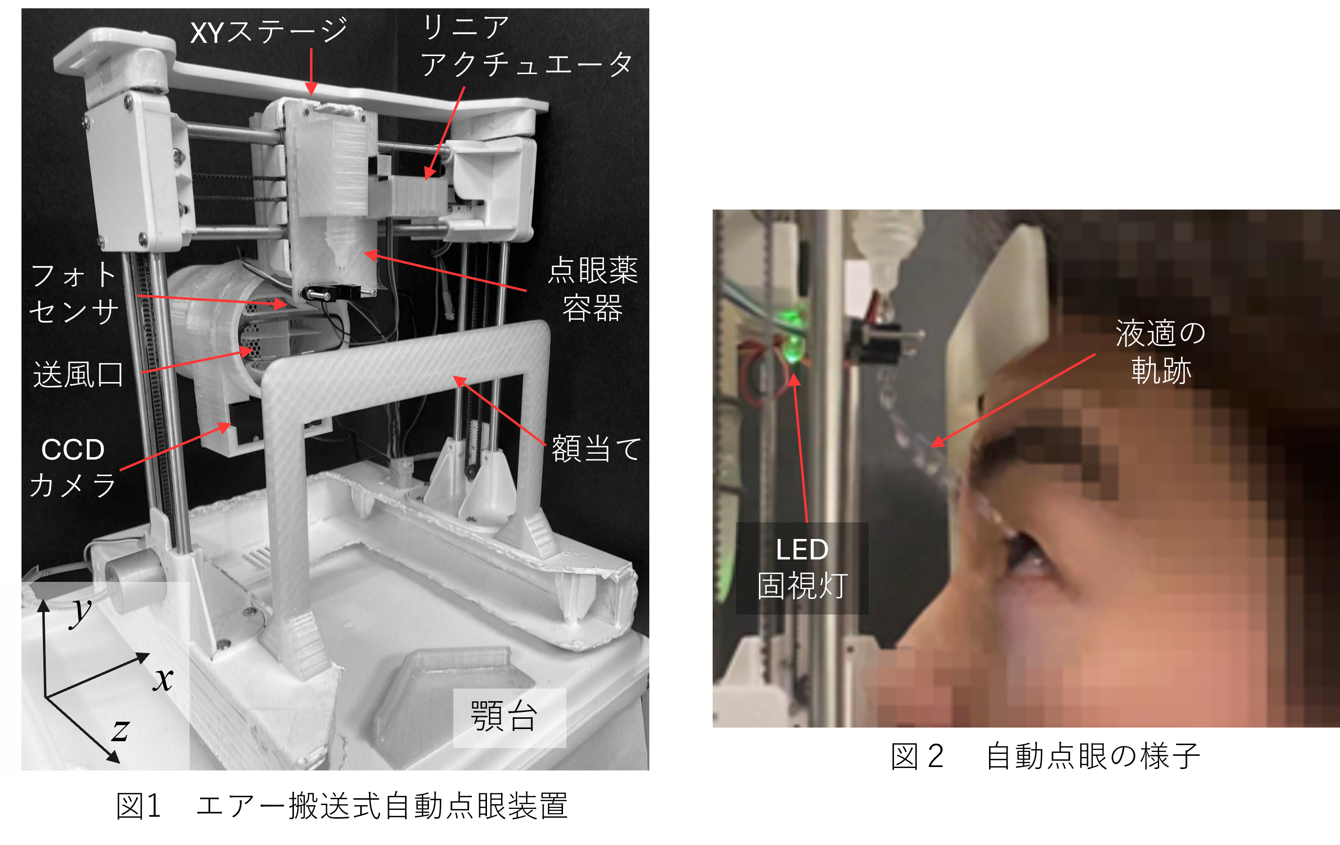
The eyes are vital organs for maintaining a healthy life. However, with age, an increasing number of people experience visual impairments, and in Japan, glaucoma is considered one of the most common eye diseases. Eye drops are essential in the treatment of glaucoma. However, a survey conducted overseas reported that only 8.6% of patients were able to apply eye drops correctly. For elderly individuals, or those with limited mobility in their hands, arms, or neck, applying eye drops can be particularly challenging. To address this issue, a device is being developed that allows eye drop application while facing forward, without requiring fine hand movements or tilting the head backward (Fig. 1). The device utilizes a mechanism in which a small stream of air is applied from the side to guide the droplet toward the eye. The trajectory of the eye drop can be determined by solving a second-order differential equation. Although this air-blown delivery method involves a slightly more complex structure compared to conventional gravity-based systems, it allows users to apply eye drops comfortably and reliably while seated—particularly beneficial for individuals with limited neck or hand mobility (Fig. 2).
Keywords
Theme2:Medication Administration Monitoring Device
Overview
To prevent missed doses and medication errors, a device has been developed to help patients and caregivers manage medication intake more easily, while also enabling healthcare professionals to monitor usage status. Proper medication management is essential, as issues such as forgotten doses or overdosing can lead to serious health risks. This device allows users to track and verify which medications were used and in what quantities.
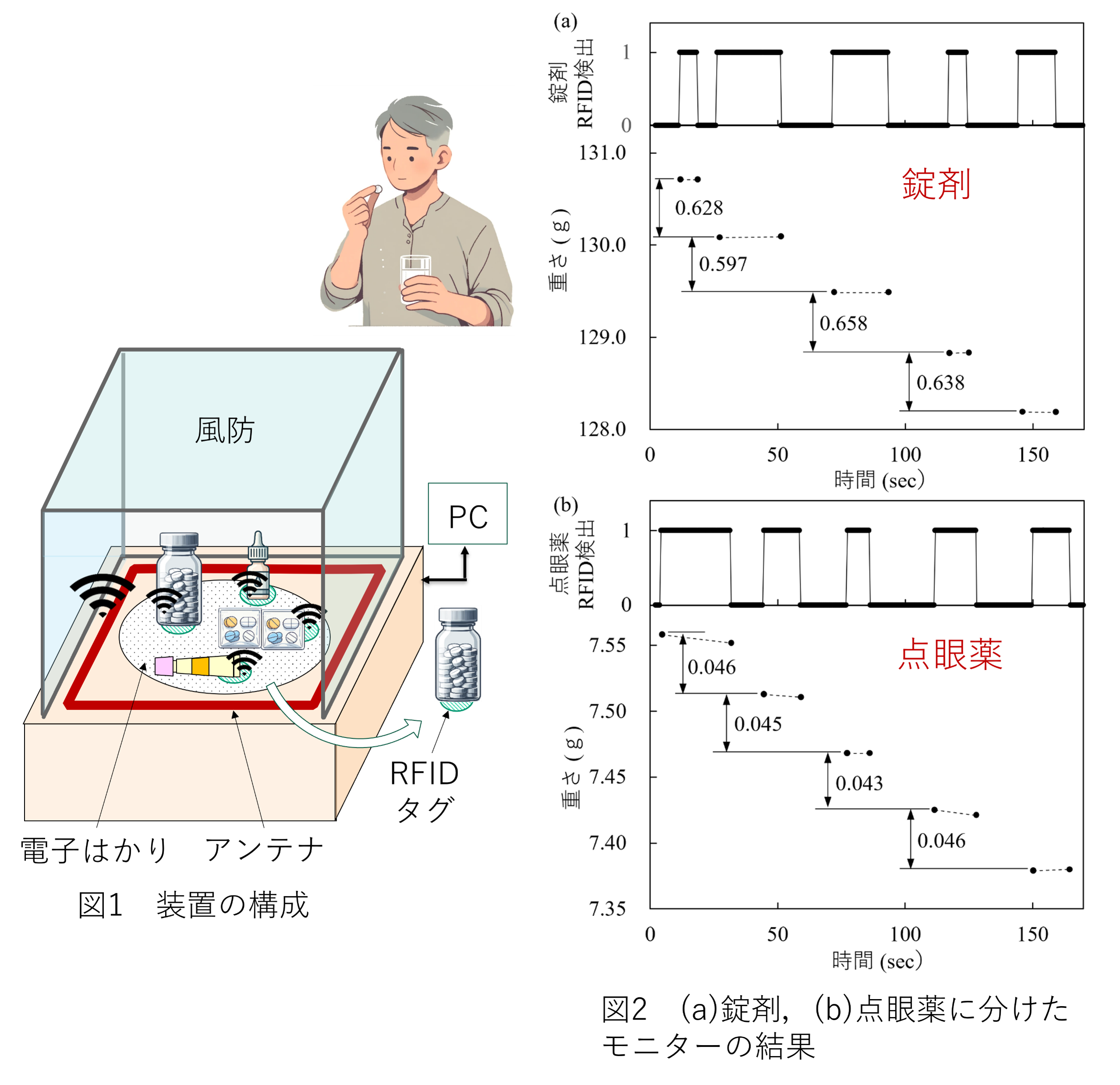
The system combines RFID (Radio-Frequency Identification) technology with an electronic scale, enabling real-time monitoring of medication type, dosage, and user identity (Fig. 1). By adding weight measurement capabilities to conventional RFID systems, the device can now support not only tablets and pre-packaged doses, but also liquid and semi-liquid medications such as eye drops and ointments, which were previously difficult to manage (Fig. 2). When used in conjunction with RFID-tagged user plates, the device can record medication usage on a per-user basis. The recorded data is stored on the cloud and can be visualized in graphical form via an application. It is also available for download as a usage log or record sheet.
Keywords
Theme3:Optical Coherence Tomography (OCT)
Title of class
Fundamental Experiments of Electrical, Electronic and Information Engineering
Analytical Electromagnetics II
Quantum Mechanics II
Magnetism
Advanced Materials for Electronics I
Materials for Electronics
Advanced Electronic Materials 1