
Yamane, Keisuke
| Affiliation | Department of Electrical and Electronic Information Engineering |
|---|---|
| Title | Associate Professor |
| Fields of Research | Semiconductor engineering, crystal engineering |
| Degree | Toyohashi University of Technology |
| Academic Societies | Japan Society of Applied Physics |
| yamane@ee Please append ".tut.ac.jp" to the end of the address above. |
|
| Laboratory website URL | http://www.int.ee.tut.ac.jp/oeg/ |
| Researcher information URL(researchmap) | Researcher information |
Research
There is no doubt that an enormous amount of information produced by internet industry and advanced sensing technology has improved our lives. Si-LSIs are now playing an important role as key devices to process such information. Since Si-LSIs are operated by a time-series / serial processing system with electrical signals, their performance is now unlikely to improve substantially due to a physical limitation. In this study, we propose the monolithic integration of Si-LSIs and light emitting devices / photodetectors for the realization of next-generation LSIs. If a new parallel processing system is established by introducing the optical inter/intra connections, ultra-high speed processing and new sensing systems are expected.
Theme1:Monolithic Opto-Electronic Integrated System by Silicon /III-V Nitride Semiconductor Heterostructure
Overview
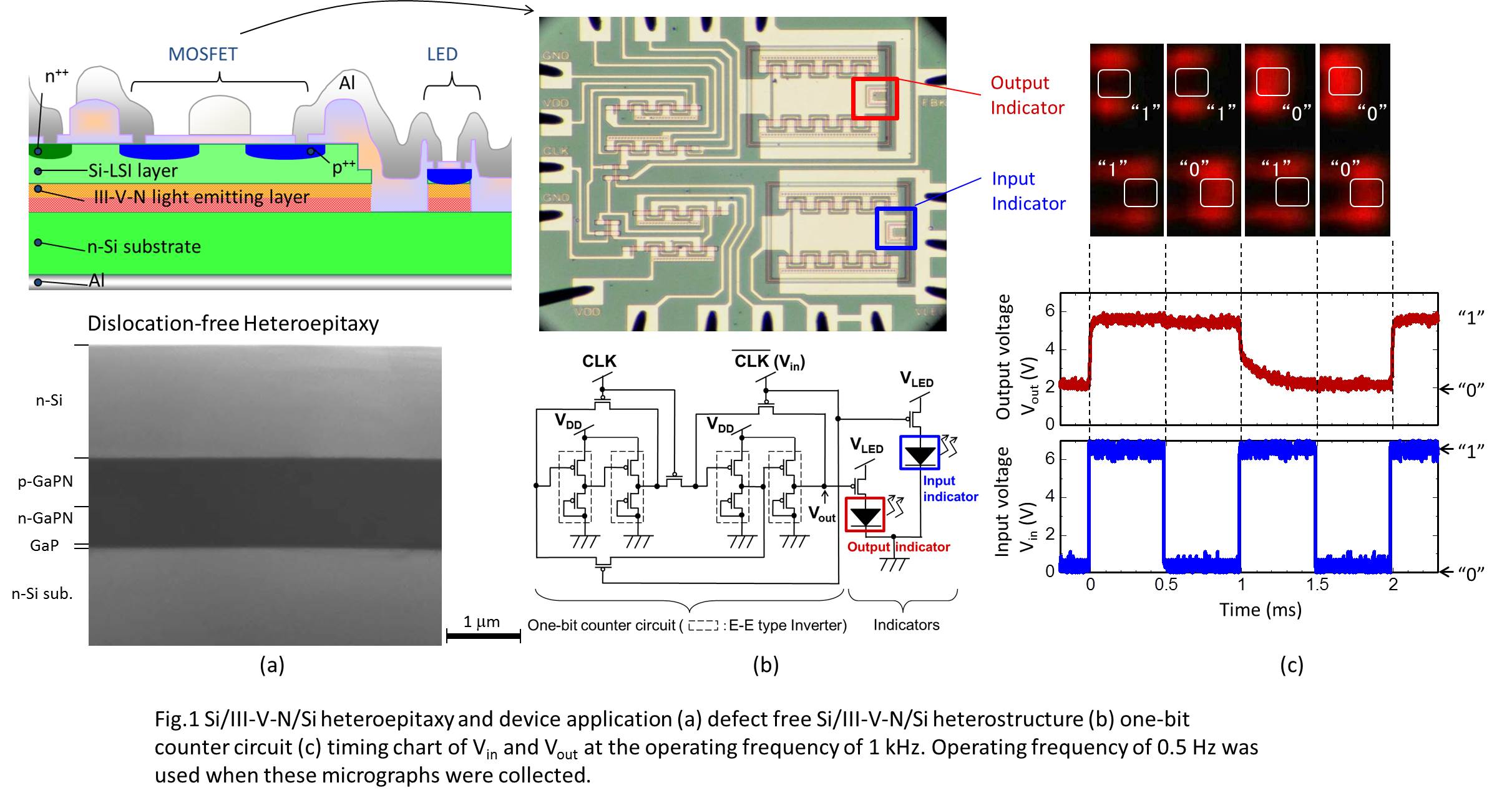
One of our targets is monolithic opto-electronic integrated system, which offers advantages of compatible fabrication process of Si-LSIs and high efficiency/reliability of light emitting devices. The figure shows a prototype of opto-electronic integrated circuits [1]. We developed the growth sequence of a defect free Si-LSI and III-V-N light-emitting layers on Si substrate [2] (left). Then we fabricated a bit counter circuit (center) and demonstrated the monolithic integration of bit counter circuits and light emitting devices (right). Improvement of efficiency of light emitting device, integration of photodetectors and circuit design are future work.
[1] K. Yamane, K. Noguchi, S. Tanaka, Y. Furukawa, H. Okada, H. Yonezu, A. Wakahara, “Operation of monolithically-integrated digital circuits with light emitting diodes in lattice-matched Si/III-V-N/Si heterostructure”, Applied Physics Express 3 (2010) 074201.
[2] K. Yamane, T. Kawai, Y. Furukawa, H. Okada, A. Wakahara, “Growth of low defect density GaP layers on Si substrates within the critical thickness by optimized shutter sequence and post growth annealing” , Journal of Crystal Growth 312 (2010) 2179.
Title of class
Electrical and Electronic Information Engineering Laboratory II