
Pei Loon Khoo

| Affiliation | Department of Mechanical Engineering |
|---|---|
| Title | Assistant Professor |
| Fields of Research | Materials Engineering / Solid-state Electrochemistry/ Thin Film Science and Technology |
| Degree | Doctor of Engineering (Toyohashi University of Technology) |
| khoo@me Please append ".tut.ac.jp" to the end of the address above. |
|
| Laboratory website URL | http://tf.me.tut.ac.jp/index.html |
| Researcher information URL(researchmap) | Researcher information |
Research
Ubiquitous, photoactive, metal oxide (MO) thin film semiconductors prepared by electrochemical means possess the most promising attributes for being low-cost candidates in future applications in the field of photovoltaics (PV) and photoelectrochemical (PEC) water splitting. Advantages of such thin film MOs are scalability, ease of morphology control and abundance, which will ultimately contribute to achieving grid parity. Our research group is focused on the fundamental studies and electrochemistry science of earth-abundant MOs, especially Zinc Oxide (ZnO), Cuprous Oxide (Cu2O), and Cupric Oxide (CuO) in the applications of PV and PEC devices.
Theme1:Improvements on the Electrochemically Prepared Copper Oxide Photovoltaic Device
Overview
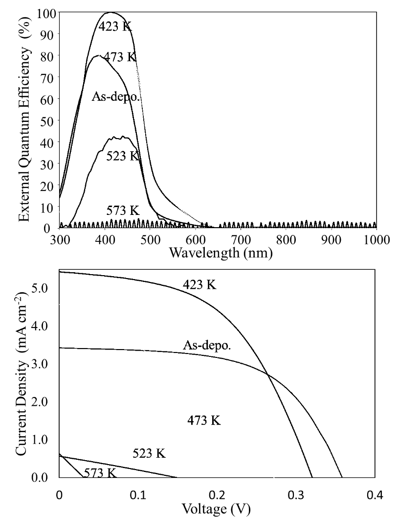 Figure 1. The effect on the EQE and I-V characteristics of n-ZnO/p-Cu2O photovoltaic devices under different annealing temperatures
The theoretical power conversion efficiency of Cu2O with the bandgap energy of 2.1 eV is approximately 20%, but current developments showed that the efficiency has left much to be desired. Our group investigates the limiting factors of such PVs, based on solid state physics.
Based on established technology of electrochemical fabrication of n-ZnO/p-Cu2O in this laboratory, annealing was proposed as a performance improvement method to lessen carrier scattering defects in the light-absorbing layer. Promising results were attained with a 20% increase in maximum external quantum efficiency (EQE) under optimum annealing temperature of 423 K, which corresponded to a dramatic improvement in charge collection.[1] The mechanism was also elucidated which was evidenced by Hall measurement, showing an increase in carrier mobility due to decreased scattering defects. Also, by combining Cu2O and CuO via rapid thermal annealing of electrochemically prepared Cu2O, a light-absorbing layer with different bandgap energies was formed and the absorption edge of the photoactive layer was successfully extended which displayed an augmented EQE range.[2]
A further improvement for charge collection for wavelengths around 500 nm is being attempted by introducing nano-patterning during electrochemical preparation to further enhance the optical and electrical characteristics of the heterojunction.
Selected publications and works
[1] Pei Loon Khoo, Yuuki Kikkawa, Kenta Satou, Tsutomu Shinagawa, and Masanobu Izaki. “Improvements in External Quantum Efficiency of Electrochemically constructed n-ZnO/p-Cu2O Photovoltaic Devices by Rapid Thermal Annealing”, Thin Solid Films, 653 (2018),158-164
[2] Masanobu Izaki, Kazuma Fukazawa, Kenta Sato, Pei Loon Khoo, Masakazu Kobayashi, Akihisa Takeuchi, and Kentaro Uesugi. “Defect Structure and Photovoltaic Characteristics of Internally Stacked CuO/Cu2O Photoactive Layer Prepared by Electrodeposition and Heating.” ACS Appl. Energy Mater. 2019, 2, 7, 4833-4840
Keywords
Theme2:Novel Cu2O/CuO Continuously Stacked Electrodeposition and Its Applications
Overview
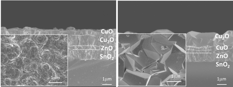 Figure 2. Directly-stacked Cu2O/CuO layers by deposition potential control from aqueous solution containing cuprous-tartrate complex
While inclusion of multiple bandgap energies in the light-absorbing layer can be achieved by thermal oxidation of the electrochemically-prepared Cu2O films creating Cu2O/CuO photoactive layers, our group have recently reported the successful fabrication of both Cu2O and CuO layers from a single aqueous solution by controlling the deposition potentials.[1] This new method may solve many complications faced in thermal oxidation such as avoiding formation of nanopores and defects, and open doors to fabrication of various composite copper oxide layers which were impossible until now. Our group is currently investigating the various possibilities enabled by this novel technique in PV and PEC water splitting applications.
Selected publications and works
[1] Masanobu Izaki, Takayuki Koyama, Pei Loon Khoo, and Tsutomu Shinagawa. "Light-Irradiated Electrochemical Direct Construction of Cu2O/CuO Bilayers by Switching Cathodic/Anodic Polarization in Copper(II)-Tartrate Complex Aqueous Solution", ACS Omega 2020, 5, 1, 683-691