
ここからコンテンツです。
Enabling disease diagnosis and viral detection with ultra-sensitive microsensors
Kazuhiro Takahashi
Professor Kazuhiro Takahashi is working on the development of ultra-compact biosensors that can be used to diagnose diseases, and more. What makes these sensors special is the use of optical interference to measure mechanical changes that occur when the substance to be measured is absorbed onto a suspended thin film on a microchip. The sensors will enable cancer screening, virus detection, and other functions to be performed by the compact device with a high level of sensitivity as well as with ease. In addition, Professor Takahashi is seeking to apply this mechanism to the development of devices that can detect virus particles in the air.
Interview and report by Madoka Tainaka
Microchips play a useful role in biomarker testing and beyond
In recent years, disease-specific proteins (biomarkers) in the blood, such as prostate-specific antigen (PSA) and carcinoembryonic antigen (CEA), have been measured during medical checkups and other health exams to help screen for diseases. Since biomarkers can be measured from a tiny amount of blood, they are an extremely useful indicator linked to early diagnosis and treatment of diseases. Until now, however, it has been necessary to examine each individual biomarker using bulky equipment, such as biochemical analyzers, and testing can only be conducted at certain facilities. By detecting biomarkers with a microchip, and using a smartphone to carry out the analysis, Professor Takahashi hopes to enable users to manage their health at home and elsewhere, at an affordable price.
"We already know about various kinds of disease-specific biomarkers, and research has identified specific proteins involved in serious cases of COVID-19. If we were able to test for these at home or in a rest home, using our smartphones, it would be possible to provide priority treatment to patients who have higher values. Since our sensors not only examine blood, but also saliva, urine, and exhaled breath, I think they can be applied in a wide range of areas, such as health care and prevention of infectious diseases."
Professor Takahashi and his team are developing a semiconductor microchip that will unlock the potential of such a visionary device. Above the chip sits a thin film, engineered to adsorb only the molecule that needs to be measured (modified chemically to adsorb only a specific substance, such as a receptor), and the device detects the mechanical change that occurs when the target molecule is adsorbed onto the film. The point is to form the film so that it floats above the substrate of the semiconductor.
"In other words, there is a tiny gap of less than one micrometer between the semiconductor and the film. Now, for a polymer film that adsorbs a biomarker, the thickness of the film will be about 100 nanometers. When molecules attach to this film, since each molecule is electrically charged, the molecules repel each other, and the film naturally expands into a dome shape. In other words, the film deforms due to the stress caused by the adsorption of molecules. To facilitate this deformation, the film must be as thin as possible, and there needs to be a gap between the semiconductor and the film. Then, by measuring the degree of deformation, you can determine how much of the target molecule has been adsorbed."
Enhanced sensitivity through sensing with optical interference
Professor Takahashi is also working on the detection of virus and gas molecules, which are even smaller than biomarkers. What they are measuring here is the mass of the molecule.
"To measure the molecular mass, voltage is applied to make the film vibrate. The frequency of vibration depends on the molecular mass: When molecules such as viruses attach to the surface of the film, the mass increases, and the vibration frequency falls. By measuring this frequency, we can observe how much of the molecule has been absorbed. So in both cases we are utilizing the functionality of micro-electromechanical systems (MEMS), but we are doing so in two different ways: In one we observe the deformation of the film due to intermolecular force, and in the other we actively apply a voltage to make the film vibrate and observe the change in frequency," explains Professor Takahashi.
So how do the sensors detect the film deformation or changes in the vibration? They use the principal of optical interference. The idea is to measure an optical phenomenon called "Fabry–Pérot interference", which occurs when a film is illuminated by a monochromatic light source, such as a red laser. What makes this research unique is the use of optical interference to detect biosensors.
"Here too, the gap between the semiconductor and the film is critical. Because the wavelengths at which the beams of light reinforce each other change depending on the thickness of the gap between the semiconductor and the film—the same principle as Newton’s rings, which we studied in high school physics. In other words, as molecules are adsorbed and the film expands, increasing the thickness of the gap, the colors produced when the light is applied change. This light intensity (change in color) is detected using a semiconductor—a complementary metal oxide semiconductor (CMOS)—image sensor."
With CMOS image sensors, which are also used in smartphone cameras, if a different film is prepared for each pixel, a 10-megapixel CMOS sensor, for example, can in principle detect 10 million different substances. This means that it would also be possible to view the types of molecules adsorbed onto each film (pixel) as an image.
"The conventional method used for biosensing is to observe reactions in a solution, but since this new method allows you to observe molecules in the air it is also well suited to downsizing and integration. What’s more, the measurements can be done at a level of sensitivity more than two orders of magnitude higher than other methods," says Professor Takahashi.
He will now work toward commercializing the technology in partnership with industry.
Detection of viruses in the air
What Professor Takahashi is focusing on right now, however, is the development of an innovative sensor that can detect COVID-19 particles in the air.
"PCR testing is designed to show if the subject is infected. Since the reaction is examined in a solution, it takes time for the result to come through. But what we really need right now is 'on-the-spot' infection control. So, we’ve developed a sensor that can visualize virus particles in the air. The sensor, which tests for the presence of the virus in exhaled breath, could be used to check whether people are infected upon entering a facility or boarding an airplane, or for screening of high-risk contacts. With sensors installed at different locations, it would be possible to visualize viral hotspots and use the information to create hazard maps. So, the technology can be used to visualize risk."
This sensor adopts the same principle as the one introduced above, the main difference being that it uses an ultra-thin film with a single atomic layer. The film is only 0.34 nanometers thick. The reason for using such a thin film is that if the mass of the film is closer to that of the molecule to be adsorbed, a larger reaction—a higher level of sensitivity–can be achieved. The research team has already created a chip, in which graphene film (a sheet of carbon atoms) floats freely from the semiconductor substrate, which is more sensitive than a conventional silicon-based MEMS sensor.
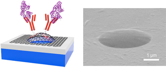
(Right) Photograph of a freestanding atomic layer graphene film.
"When a single virus particle—which weighs 100 attograms, or about 10-16 grams—attaches to the film, this alone causes the frequency of vibration to fall by as much as 100 kilohertz. This means that, in principle, the sensor can detect a single virus particle. But making something this small not easy. In particular, when modifying the antibody molecule on the graphene we need to perform the process in a solution; but even just adding it to a solution causes it to break. To solve this problem, we enhanced the strength of the graphene structure by making innovative changes to the structure of the graphene, successfully modifying the antibody molecule."
"In fact, this sensor was originally developed to detect influenza viruses. In the future, we hope to be able to test for COVID-19 and influenza simultaneously," adds Professor Takahashi.
This is exactly the kind of technology we need today; we look forward to its speedy rollout.
Reporter's Note
Professor Takahashi explains how in high school he was fascinated by rockets and space development. As a university student, he stepped unexpectedly from the macro to the micro world.
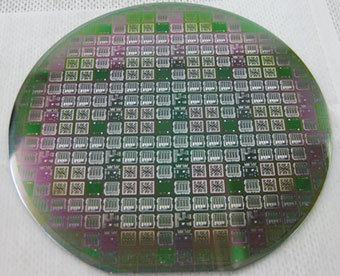
"It was while I was researching optical switches at graduate school that I learned that Toyohashi University of Technology had a fully-fledged LSI factory, and I resolved to do research there one day," recalls Professor Takahashi. All the sensors introduced in this article were developed at the university.
Furthermore, Toyohashi University of Technology has just been selected for the Ministry of Education, Culture, Sports, Science and Technology’s Initiative to Establish Next-generation Novel Integrated Circuits Centers (X-NICS). We hope that the research of Professor Takahashi and his team will spark a series of breakthroughs, helping drive the revival of Japan’s semiconductor industry.
小型の超高感度センサで病気の診断やウイルスの検知を可能に
高橋一浩教授が手がけるのは、病気の診断などに活用できる超小型のバイオセンサの開発だ。その特徴は、計測したい物質がマイクロチップ上の薄膜に吸着した際の力学的な変化を、光の干渉を使って測るというもの。これにより、がん診断のスクリーニングやウイルスの検知などを高感度に、しかも小型のデバイスで簡単に実現できるようになるという。さらにこのしくみを応用して、空気中のウイルス検知のデバイス開発にも挑んでいる。
バイオマーカーなどの検査に役立つマイクロチップ
PSA(前立腺特異抗原)やCEA(胃がん大腸がんなどの腫瘍マーカー)に代表されるように、近年、健康診断や人間ドックなどでは、血液中の病気由来のタンパク質(バイオマーカー)を測ることにより、病気の診断のスクリーニングに役立てている。ごくわずかな血液から調べることができるバイオマーカーは、病気の早期診断・治療につながる極めて有用な指標の一つだ。しかしこれまで、それぞれのバイオマーカーを大型の生化学分析装置などを使って調べる必要があり、検査できる施設が限られてきた。高橋教授はこれをマイクロチップで検出し、解析にスマートフォンを利用することで、家庭などで安価に健康管理を行えるようにしたいと語る。
「現在、さまざまな種類の病気由来のバイオマーカーが知られていますが、そのなかには、新型コロナウイルスの重症化に関わる特定のタンパク質も報告されています。これを家庭や療養施設などで、スマートフォンを使って検査できれば、数値が上がってきた人を優先して治療することもできるでしょう。我々のセンサは、血液だけでなく、唾液や尿、呼気なども調べることができるため、ヘルスケアや感染症の予防などに幅広く応用できると考えています」
この夢のデバイスの可能性を拓くのが、高橋教授らが開発する半導体のマイクロチップだ。これは、チップの上に測りたい分子を特異的に吸着するような工夫(レセプターなど、特異な物質のみを吸着できる化学的な修飾)を施した薄膜を被せ、対象の分子が膜に吸着した際に生じる力学的な変化を検出するというもの。ポイントは、半導体の基板上に膜を浮かせた状態で形成することにある。
「つまり、半導体と膜の間に1マイクロメートル以下のわずかに隙間があるんですね。ちなみに膜の厚さは、バイオマーカーを吸着する高分子の膜なら100ナノメートル程度です。この膜に分子がつくと、それぞれの分子が電荷を持つことから、互いに反発し合う力が働き合って、膜が自然にドーム状に膨らみます。つまり、分子が吸着したことによる応力によって、膜が変形するのです。この変形を促すために、膜はできるだけ薄く、そして半導体と膜の間に隙間が必要なわけです。そして、この変形の度合いを検出することで、対象となる分子がどれくらい吸着したのかを検出できる、というしくみです」
光の干渉を使ったセンシングで高感度に
さらに高橋教授は、バイオマーカーよりもさらに小さいウイルスやガスなどの検出にも取り組む。このときに測るのは分子の質量だ。
「分子の質量を測る際は、電圧をかけて膜を振動させます。膜の振動の周波数は質量に依存しますが、膜の表面にウイルスなどの分子が付着して質量が増えると、周波数が下がります。これを調べることで、どれくらいの量の分子が吸着したのかがわかります。つまり、同じMEMS(Micro Electro Mechanical Systems:微小電気機械システム)の機構を使いながら、分子間の応力による膜の変形を見る場合と、積極的に電圧をかけて膜を振動させてその周波数の変化を見る場合と、二つのパターンを採用しているというわけですね」と高橋教授は説明する。
では、どうやって膜の変形や振動の変化を検出するのか。このとき用いるのが光干渉の原理だ。膜に赤色レーザーなどの単波長を照射した際に生じる「ファブリペロー干渉」という光の作用を計測するという。バイオセンサの検出に光の干渉を使うところに、この研究の独自性がある。
「ここでも半導体と膜の間の隙間がカギを握ります。というのも、高校の物理で習ったニュートンリングと同じ原理なのですが、半導体と膜の隙間の長さによって強め合う光の波長が変わるからです。つまり、分子が吸着して膜が膨らんで隙間の距離が長くなれば、光を照射した際に観測される色が変化します。この光の強度(色の変化)を半導体、すなわちCMOS(Complementary Metal Oxide Semiconductor)イメージセンサ検出します」
CMOSイメージセンサは、スマートフォンのカメラなどにも搭載されているセンサだが、たとえば1000万画素のCMOSセンサであれば、1画素ごとに異なる膜をそれぞれ用意すれば、原理的には1000万種類の物質を検出できることになる。かつ、どの膜(画素)にどれくらいの分子が吸着したのかを画像として見ることができる、というわけだ。
「現状のバイオセンシングは溶液の中で反応を見る方式が主流ですが、この方法を使えば空気中での観察が可能なうえ、小型化や集積化にも適しています。しかも、他の方式に比べると二桁以上も高感度に測ることができるのです」と高橋教授。
今後は、製品化に向けて産学連携を進めていくという。
空気中のウイルスの検出に
一方、現在、高橋教授が注力しているのが、新型コロナウイルスを空気中でそのまま検出できる画期的なセンサの開発だ。
「PCR検査は、感染したかどうかを調べるものですよね。溶液中の反応を調べるため、結果が出るまでに時間もかかります。しかし、いま求められているのは、むしろその場でできる感染予防でしょう。そこで我々が開発したのが、空気中のウイルスを可視化できるセンサです。これは、センサに呼気を吹きかけることでウイルスの有無を調べることができるというもので、施設内への入館や機内への搭乗の際に感染していないかどうかを調べたり、濃厚接触者のスクリーニングなどに活用したりできます。また、各所にセンサを配置しておけば、ウイルスの多い場所を可視化でき、ハザードマップにも役立てられる。つまりリスクの見える化が可能になるわけです」
このセンサも先述したものと原理は同じだが、大きなちがいは原子一層の極薄の膜を用いることにある。厚さはわずか0.34ナノメートル。これほど膜を薄くする理由は、膜の質量を吸着する分子の質量に近づけることで大きな反応が得られる、つまり感度を高めることができるからだ。すでにグラフェン(炭素原子でてきたシート)の膜を半導体の基板から浮かせて自立させたチップを作製し、従来のシリコンを使ったMEMSセンサに比べて、より優れた感度を実現している。
「ウイルス1個の質量は100アトグラム、すなわち10-16ほどですが、ウイルスが1個ついただけで膜の振動の周波数が100キロヘルツ程度下がります。つまり、このセンサを使えば、原理的にはウイルス1個から検出できることになります。もっともこれだけ小さなものをつくるのは容易ではありません。とくに、グラフェン上に抗体分子の修飾をつける際に溶液中で処理する必要があるのですが、溶液に入れただけで壊れてしまう。そこで、グラフェンの構造に工夫を凝らすことで強度を高めて、抗体分子の修飾に成功しました」
実はこのセンサは、もとはインフルエンザの検出用に開発したものなのだという。「今後は、コロナとインフルの同時検出も実現していきたいと思います」と高橋教授。
まさにいますぐに求められている技術であり、迅速な社会実装に期待したい。
(取材・文=田井中 麻都佳)
取材後記
高校時代はロケットや宇宙開発に憧れていたという高橋教授。大学では思いがけず、マクロとは真逆のミクロの世界に携わることになった。
「大学院で光スイッチの研究をしていたのですが、このときから、豊橋技科大に本格的なLSI工場があることを認識していて、いつか豊橋で研究をしたいと思っていたのです」と高橋教授。今回、記事中で紹介したセンサもすべて学内でつくったという。
なお、豊橋技科大は今年度、文部科学省の「次世代X-nics半導体創生拠点形成事業」に採択されたところだ。ぜひここから、高橋教授らの研究に続く画期的な成果が次々に生まれ、日本の半導体産業の巻き返しに貢献していってほしい。
Researcher Profile

Kazuhiro Takahashi
Kazuhiro Takahashi received PhD degree in 2008 from The University of Tokyo, Tokyo, Japan. He started his career at Institute of Industrial Science, The University of Tokyo as a postdoc researcher. Since he started his career at Toyohashi University of Technology as an assistant professor in 2009, had been involved in the development of CMOS-MEMS sensors and actuators for optical and biological applications. He is currently a professor at Electronics-Inspired Interdisciplinary Research Institute (EIIRIS).
Reporter Profile

Madoka Tainaka
Editor and writer. Former committee member on the Ministry of Education, Culture, Sports, Science and Technology Council for Science and Technology, Information Science Technology Committee and editor at NII Today, a publication from the National Institute of Informatics. She interviews researchers at universities and businesses, produces content for executives, and also plans, edits, and writes books.
ここでコンテンツ終わりです。