
ここからコンテンツです。
Expression of Stop Bands in Forward Volume Spin Waves
Contribution to the realization of super low-power spin wave integrated circuits By Taichi Goto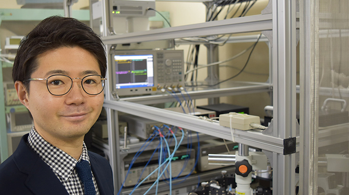
A research group led by assistant Professor Taichi Goto at Toyohashi University of Technology have, for the first time in the world, demonstrated “stop bands” that prevent propagation of specific frequency components of "forward volume spin waves." Forward volume spin waves are transmitted through magnetic insulators without the flow of current, and are expected to be applied to the next generation of integrated circuits (ICs). Furthermore, among the spin waves that have been confirmed, forward volume spin waves are the most suitable for information transmission in IC chips, and there are high expectations for their application. However, until now, noise in forward volume spin waves was large, and the stop bands, which are one of the basic physical phenomena, could not be observed. In this demonstration, a magnetic insulator was combined with metal to suppress the noise in forward volume spin waves, and the expression of stop bands was confirmed experimentally.
In recent years, electronic devices using semiconductor materials have had difficulty in responding to the demands of the rapidly growing information society. For example, due to increases in energy density due to increased integration, chip temperatures have become high, causing defects. Therefore, the development of spin wave IC chips which can process information not by moving electrons themselves but by transmitting spin only, greatly reducing the generation of heat, is attracting attention.
Specifically, spin waves traveling through magnetic insulators have the advantage of low energy loss and long-distance transmission. Furthermore, among the spin waves whose existence has been confirmed, forward volume spin waves that transmit in all directions are said to be most suited for ICs because they can be wired diagonally or in curved shapes as well as linearly. On the other hand, these forward volume spin waves are noisy, and several fundamental spin wave phenomena have not yet been demonstrated. Demonstration of these fundamental principles is indispensable for the development of IC chips and has become an important issue.
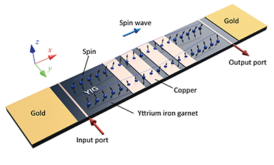
Now a research group led by Taichi Goto, of Toyohashi University of Technology, has successfully combined an Yttrium iron garnet (YIG) – an oxide single crystal well known as a magnetic insulator – with two metals (gold and copper) to suppress noise. Through this approach the research team was able to confirm the expression of stop bands in forward volume spin waves experimentally for the first time in the world. In this research, firstly, a system that could simulate the propagation of spin waves was prepared using a three-dimensional model (Figure 1) with the same scale as real spin waves. Using this system, a sample structure was determined where noise was small and the "stop bands," which are one of the fundamental spin wave phenomena, was confirmed. A stop band is a phenomenon that does not allow spin wave components of a specific frequency to pass through, and stop bands are also expressed in other waves such as electromagnetic waves including light.
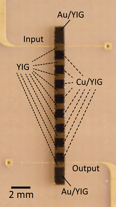
Next, samples were made to be as close as possible to the simulation. Figure 2 shows a sample prepared using materials from Shin-Etsu Chemical Co., Ltd. Both ends of the yttrium-iron garnet (which was processed into a wire shape) were covered with gold film to suppress noise generation, and by arranging a copper film in stripes like a pedestrian crossing, the research team tried to hinder the propagation of specific frequencies. Spin waves of various frequencies were passed through this sample and the transmission characteristics were measured.
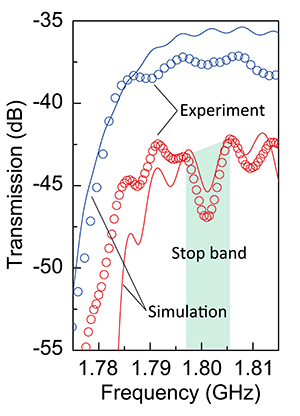
As a result, the “stop bands” were confirmed as shown in Figure 3. By comparing these with the characteristics of samples without stripe-arranged copper, it can be seen that the expression of stop bands is due to the stripe-arranged copper. Also, the experimental results and the calculation results are in good agreement. From this, the results can be predicted by simulation before experiment, leading to the potential for efficient spin wave IC development.
The promising results of this research can be used for applications such as spin wave filters in spin wave IC chips in the future. In addition, they can also be used to slow down the transmission speed of spin waves and to control the direction of travel, contributing to the development of smaller chips capable of more dense information processing.
This research was jointly conducted by Assistant Professor Taichi Goto, PhD student Kei Shimada, Associate Professor Yuichi Nakamura, Professor Hironaga Uchida, and Professor Mitsuteru Inoue of the Toyohashi University of Technology. Additionally, the samples used for the experiment were prepared under a joint research initiative with Shin-Etsu Chemical Co., Ltd.
This research was supported by JST PRESTO Number JP JPR 1524 and JSPS KAKENHI Nos. 17K19029, 16H04329, 26220902.
Reference
Taichi Goto, Kei Shimada, Yuichi Nakamura, Hironaga Uchida and Mitsuteru Inoue (2019). One-dimensional magnonic crystal with Cu stripes for forward volume spin waves, Physical Review Applied.
https://link.aps.org/doi/10.1103/PhysRevApplied.11.014033
前進体積スピン波のストップバンドの発現を実証
超低消費電力なスピン波集積回路実現に貢献By 後藤 太一
豊橋技術科学大学の後藤太一 助教らは、「前進体積スピン波」の特定の周波数成分の伝搬を妨げる「ストップバンド」を実証しました。前進体積スピン波は、電流を流さずに磁性絶縁体中を伝わることから、次世代の集積回路への応用が期待されています。また、確認されているスピン波の中で集積回路チップ内の情報伝達に最も適しており、応用が強く期待されているものです。しかし、これまで、前進体積スピン波のノイズは大きく、基本的な物理現象の1つであるストップバンドが観測できていませんでした。今回の実証では、磁性絶縁体と金属を組み合わせ、前進体積スピン波のノイズを抑制し、ストップバンドの発現を実験で確認しました。
近年の半導体材料を利用した電子デバイスは、高集積化によるエネルギー密度の増加に伴い、チップの温度が高くなり、不具合を生じるなどして、急成長する情報化社会からの要求に答えることが難しくなってきています。そこで、電子自体は移動せずスピンだけを伝えることで情報処理を行い、熱の発生が大幅に低減可能なスピン波集積回路チップの開発が注目を集めています。
この中でも、磁性絶縁体中を伝わるスピン波は、エネルギーの損失が小さく、長距離伝送が可能という利点を持っています。さらに、存在が確認されているスピン波の中でも、あらゆる方向に伝わる前進体積スピン波は、直線状の配線だけでなく、斜めや曲線の配線が可能なため、最も集積回路に適すると言われています。その一方で、この前進体積スピン波はノイズが大きく、いくつもの基本的なスピン波の現象が実証されていませんでした。このような基本原理の実証は、集積回路チップの開発には必要不可欠であり、重要課題となっていました。
今回、豊橋技術科学大学の後藤太一らは、酸化物で磁性絶縁体として有名な単結晶のイットリウム鉄ガーネット(Yttrium iron garnet、 YIG)と2つの金属(金と銅)を組み合わせ、ノイズを抑制し、前進体積スピン波のストップバンドの発現を実験で確認しました。本研究では、最初に、現実と同じスケールの三次元モデル(図1)を用いて、スピン波の伝搬がシミュレーションできるシステムを整えました。これを用いて、ノイズが小さく、基本的なスピン波の現象の一つである「ストップバンド」が発現する試料構造を決定しました。ストップバンドとは特定の周波数のスピン波成分を通さない現象であり、光を含む電磁波など他の波についても表れるものです。
次に、このシミュレーションと、できる限り同じ試料を作製しました。図2が信越化学工業株式会社から材料提供を受け作製した試料であり、線状に加工したイットリウム鉄ガーネットの両端を金膜で覆うことでノイズ発生を抑え、銅の膜を横断歩道のように周期配列することで特定の周波数の伝搬を妨げるようにしました。
この試料に、さまざまな周波数のスピン波を流し、透過特性を測定したところ、図3のように、ストップバンドが発現しました。周期配列した銅がない試料の特性と比べると、ストップバンドの発現が周期配列した銅による影響であることが分かります。また、実験結果と計算結果がよく一致しました。このことから、実験をする前にシミュレーションで結果が予測でき、効率的なスピン波集積回路開発に繋がると期待できます。
今回得られた成果は、将来のスピン波集積回路チップの中では、スピン波のフィルター等として使うことができます。他にも、スピン波の伝わる速度を遅くしたり、進む方向をコントロールしたりすることにも使うことができ、より小型で、高密度で情報処理を行うチップの開発に寄与します。
本研究は、豊橋技術科学大学の後藤太一 助教、島田馨 博士前期課程生、中村雄一 准教授、内田裕久 教授、井上光輝 教授らが共同で行ったものです。また、実験に用いた試料は、信越化学工業株式会社との共同研究のもと作製されました。
Researcher Profile

| Name | Taichi Goto |
|---|---|
| Affiliation | Department of Electrical and Electronic Information Engineering |
| Title | Assistant Professor |
| Fields of Research | Magnetics / Optics/ Photonics/ Nanotechnology/ Spintronics/ Magnonics |
ここでコンテンツ終わりです。