
ここからコンテンツです。
Semiconductor chip that detects exhaled gas with high sensitivity at room temperature
Toward the realization of IoT chemical sensors capable of diagnose diseases through breath testing By Toshiaki Takahashi
Doctoral student Toshiaki Takahashi*, associate professor Kazuhiro Takahashi, and their research team of the Department of Electrical and Electronic Information Engineering at Toyohashi University of Technology developed a testing chip using semiconductor micro-machining that can detect volatile gasses in exhaled breath at the ppm level at room temperature. A polymer that expands and contracts when gas is absorbed is formed on a flexibly deformable nanosheet, and the amount of deformation that occurs when a target gas is absorbed is measured, allowing gas to be detected at high sensitivity. The testing chip which is no more than a few square millimeters in area thanks to semiconductor micro-machining technology, is expected to contribute to telehealth as an IoT gas sensor that can easily be used in the home for breath tests.
*The authors' affiliation and title is at the time this research was conducted.
When measuring specific molecules in the breath and blood as an index for identifying the existence and degree of progression of various illnesses, there are several methods to choose from. Amongst these methods, non-invasive measuring by breath testing has emerged as a promising and patient-friendly option. It has been identified that volatile organic compounds found in exhaled breath will increase in concentration in cases of diabetes, renal failure, lung cancer, and other illnesses. Consequently it can be reasonably be expected that these laboratory markers will be measured for use in patient screenings.
Up to now semiconductor gas sensors have generally worked by using a film formed on a sensor whose electrical resistance and capacitance change in reaction to a gas. Measurements are then made by heating the film to several hundred degree Celsius. However, in order to reduce the resulting temperature increases in the peripheral circuits, it becomes necessary to house them in a separate structure. This in turn creates issues arising from the increased complexity of the manufacturing processes and the decrease of the integration per unit area due to the isolation of elements. In addition, the increase in power consumption caused by heating poses a problem for applications in IoT devices.
To counteract these problems, the research team developed a new type of sensor that forms a polymer material which expands and contracts when gas molecules are absorbed onto a thin, flexibly deformable nanosheet. It then measures the amount of the target gas absorbed in terms of the amount of deformation of the sheet. The proposed sensor uses the interferometric property of light intensification through a narrow gap to determine gas adsorption in terms of color change. As a result of this technology, it is now possible to create a testing chip that can measure gas at room temperature without a heating mechanism.
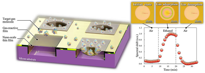
Also, this sensor can increase sensitivity without increasing area because of the formation of a narrow, sub-micron air gap of up to a few hundred nanometers between the thin flexible nanosheet and the semiconductor substrate. However, it was very difficult to merge the thin nanosheet above the sub-micron air gap while forming the gap, and it was necessary to develop a new manufacturing process to achieve the structure.
Therefore, the team focused on the strong adhesive properties of the thin nanosheet when heat and pressure are applied. A new manufacturing process was introduced where two different silicon substrates are adhered, and then the substrate on one side is removed to create a sensor structure with a sub-micron air gap of about 400 nanometers. In comparison to traditional sensor structures formed with a gap of a few micrometers, the sensor response was demonstrated to have improved by 11 times, and it was possible to determine the deformation of the thin nanosheet due to gas adsorption in terms of color change.
Additionally, it was demonstrated that the testing chip that was developed can detect ethanol gas, a typical volatile organic compound, in ppm level concentrations. The lower concentration detection limit is equivalent in performance to the most sensitive semiconductor sensors that can measure at room temperature, and compared to sensors that use the same detection method, the detection performance improved by 40 times, while the area per single element was reduced to 1/150. These properties make it likely that this sensor can be used in future as part of a small, portable breath testing device.
The research team plans to demonstrate the possibility of using the semiconductor sensor they developed to detect various volatile gasses related to illnesses. Also, they aim to construct a small, portable sensor system for breath monitoring that consumes less power than traditional IoT gas sensors.
Reference
Toshiaki Takahashi, Yong-Joon Choi, Kazuaki Sawada, and Kazuhiro Takahashi, A ppm Ethanol Sensor Based on Fabry–Perot Interferometric Surface Stress Transducer at Room Temperature, Sensors.
https://doi.org/10.3390/s20236868
室温環境下で呼気ガスを高感度に検出する半導体チップを開発
呼気検査による病気診断が可能なIoT化学センサに向けてBy 高橋 利昌
豊橋技術科学大学 電気・電子情報工学専攻博士後期課程 高橋利昌*、電気・電子情報工学系 髙橋一浩准教授らは、半導体マイクロマシン技術を用いて作製したチップ上で、室温環境下において呼気に含まれる揮発性ガスをppm程度の濃度で検出可能な検査チップを開発しました。ガスを吸収した際に膨張・収縮する特性を持ったポリマーをフレキシブルに変形するナノシート上に形成し、標的ガスの吸収に伴う変形量を計測することにより、ガスの高感度検出が可能となります。半導体技術により数ミリ角のサイズで形成した検査チップは、IoTガスセンサとして、家庭において簡易的な呼気検査を行うことで、遠隔医療への貢献が期待されます。
*文中所属は本研究が行なわれた大学在籍当時のものです
様々な疾患の存在や進行度を知るための指標として、呼気や血中に含まれる特定の分子を計測する検査手法があります。その中でも呼気診断による非侵襲計測は患者の負担が少なく、有望な疾患の検査方法として近年注目されています。呼気に含まれる揮発性有機化合物は糖尿病や腎不全、肺がん等に関連して濃度が増加することが報告されており、このような検査マーカーを計測することにより、患者のスクリーニングに活用することが期待できます。
現在までに開発されている半導体ガスセンサでは、ガスに感応して電気抵抗値や静電容量値が変化する膜をセンサ上に形成し、それを数百度に加熱することで計測を行っています。しかしながら、加熱による周辺回路への温度上昇を抑制するために、加熱部から周囲を分離するための構造を別途形成する必要があり、製作工程の煩雑化や素子間分離による単位面積当たりの集積度の低下が課題として挙げられます。また、加熱による消費電力の増加により、IoTデバイスへの応用が困難となる課題がありました。
そこで、研究チームは、ガス分子の吸収により膨張・収縮する特性を持ったポリマー材料 をフレキシブルに変形するナノ薄膜上に成膜し、標的ガスの吸収量を膜の変形量として計測するセンサを開発しました。提案センサは,光が狭い隙間で強め合う干渉特性を利用して,ガスの吸着を色の変化としてとらえることができます。この技術により,加熱機構を搭載せずに室温環境下でガスの計測が可能な検査チップが実現できました。
また,本センサは変形するナノ薄膜と半導体基板の間に作られる微小な空間を数百ナノメートルサイズまで狭く形成することにより、面積を拡張することなく、感度を向上させることが可能です。しかしながら、微小な空間を形成しつつ、その上にナノ薄膜を一体化することは非常に困難であり、この構造を実現する新たな製作工程を開発する必要がありました。
そこで、ナノ薄膜が熱と圧力の印加により強固に接合する特性に着目し、異なる2つの基板を接合後、片側の基板を剥離する製作工程を新規に導入することで、400ナノメートル程度の微小な空間を有するセンサ構造を実現しました。これにより、数マイクロメートルの隙間で形成されていた従来センサ構造に対し、センサ応答が11倍程度向上することを実証し、ガスの吸着によりナノ薄膜が変形していく様子を色の変化として捉えることが可能となりました。
さらに今回開発した検査チップにおいて、典型的な揮発性有機化合物であるエタノールガスを数ppm程度の濃度で検出が可能であることを実証しました。この検出下限濃度は、室温環境下で測定可能である最も高感度な半導体センサと同等の性能を有しており、同検出方式のセンサと比較して、1素子あたりの面積は150分の1に小型化しつつ、検出性能は40倍向上していることを示しており、携帯可能な小型呼気検査装置としての応用が期待できます。
研究チームは、今後疾患に関連する様々な揮発性ガスに対して、開発した半導体センサ上で検出可能であることを実証していく計画です。また,携帯可能な小型センサシステムを構築し,従来よりも消費電力の低いIoTガスセンサとして呼気モニタリングシステムを目指しています。
Researcher Profile
| Name | Toshiaki Takahashi |
|---|---|
| Affiliation | Micron Memory Japan, G.K. |
| Title | ADTJ PI Engineer |
| Fields of Research | Micromechanics, Semiconductor devices, Gas sensors, Bio sensors |
| Degree | Ph.D. (Engineering), Toyohashi University of Technology |
| Graduated KOSEN |
National Institute of Technology, Asahikawa College |
ここでコンテンツ終わりです。