
ここからコンテンツです。
Innovating the world of MEMS by overcoming problems through ingenuity
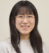
Chinatsu Kawakami
Chinatsu Kawakami completed her masters course at Toyohashi University of Technology in March 2021. Since her time as a student in a KOSEN - National Institute of Technology, she had always aspired to be involved in the development of medical devices. Her particular interest was to research MEMS (microelectromechanical systems), which are a key technology in this field. After being admitted to Toyohashi University of Technology, she joined the research lab of professor Kazuaki Sawada. She worked on the development of ion image sensors, focusing on designing a method for creating a structure that inhibits problematic ion diffusion. Additionally, she studied abroad at KAIST in South Korea where she successfully created a micrometer-sized (μm) LED probe with a 3D printer for use in optogenetics. This success was the fruit of Kawakami's originality and her serious approach to research.
In addition, she was also an active member of the inauguralclass of students to join TUT’s Global Technology Architects course, established as part of the Top Global University Project. In this capacity, she became a leading figure in on-campus, local and international activities , contributing to the globalization of TUT.
Interview and report by Madoka Tainaka
Attempting a structure that inhibits ion diffusion
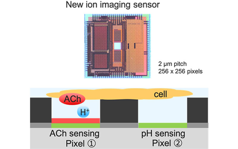
The Ion image sensor is a biosensor that combines of integrated circuit and sensor technology to directly image the distribution and movements of ions. By attaching an enzymatic membrane to the sensor and measuring the ions detected by the enzymatic reaction, it is possible to indirectly image neurotransmitters, making it an innovative sensor that will be useful for the advancement of brain science and early diagnosis of diseases.
At Toyohashi University of Technology, advancements in this research have been primarily led by professor Kazuaki Sawada, the inventor of the ion image sensor. He has already successfully visualized multiple neurotransmitters released from hippocampal slices taken from mice. Now, through industry-academia collaboration, the company is accelerating its efforts to commercialise the technology.
One of the key challenges in developing this ion image sensor has been ion diffusion. Chinatsu Kawakami, who started working on creating a sensor structure under professor Sawada, explains the reason in the following way.
"In order to measure the ion concentration, the measurement must be made in a solution. However, the ions diffuse in the solution. Therefore, the problem was that localized imaging could not be performed. Only an image with a vague, blurred outline could be obtained. Recently, a sensor was finally developed that can measure at the cellular level with a 2 μm pitch, but the close proximity of the pixels increases the effect of ion diffusion. Therefore, I started to work on creating a structure that inhibits ion diffusion."
At first, the instruction from professor Sawada was to create a well-shaped structure with a 2 μm pitch and a depth of 5 μm, using the photolithography technology used to fabricate integrated circuits. An enzyme membrane is formed on the sensor, and the well-shaped structure is formed above that. Ions that react to the enzyme are held in the well, which prevents lateral diffusion and allows high-definition images to be obtained.
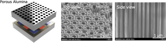
"However, even if the well-shaped pattern can be made on the surface with photolithography, the effects of light diffraction, etc., prevented the imaging of depth. Also, even minor alignment deviations would result in all of the pixels being covered by the structure, causing it to be a failure. Through trial and error, I abandoned photolithography due to its limitations, so I looked for a more appropriate materialand found it: porous alumina membrane."
Successful high-definition imaging through the adoption of a porous alumina membrane
The porous alumina membrane is a thin membrane material with a self-organizing nanopore arrangement. The small pores have a diameter of 180 to 400 nm. Also, the deciding factor for the adoption of this material is its biocompatibility, as the membrane is used in biosensors.
Kawakami explained, "If this could be crimped to the structure, there would be multiple holes open for each pixel, and minor alignment deviations would not be a problem. A 54 μ㎡ enzyme membrane was formed on a semiconductor. This was exposed to light, and the enzyme membrane that degrades acetylcholine (ACh) was patterned at a 64 μm pitch. The porous alumina membrane was then crimped above that. As a result of this experiment, we proved that it is possible to inhibit ion diffusion and obtain a high-definition image."
When acetylcholine was dripped on a sensor without a structure, the ions generated by the enzyme reaction diffused, and as time elapsed, the pattern disappeared. In contrast, for a sensor with a structure, the square-shaped pattern of the ACh sensor part and the surrounding hydrogen ion sensor part was maintained even after time elapsed. For confirmation, the change in electric potential of the ACh sensor part and the hydrogen ion sensor part were investigated by plotting the electric potential, and it was understood that ions were only detected by the ACh sensor part when the sensor had a structure.
"Ultimately, we were successful in imaging with an enzyme membrane with a 16 μm pitch. Since the size of a single cell ranges from several μm to 50 μm, we were able to show that multiple types of neurotransmitters released by a single cell can be detected in high definition."
In the future, professor Sawada’s research team will will study the optimal thickness of the alumina film and increase the number of neurotransmitters that can be detected through animal experiments in collaboration with companies and research institutes.
Successful creation of micro-LED probes with a 3D printer
In actuality, Kawakami had difficulty coming up with the process for the structure during her fourth year as an undergraduate. She arrived at the idea for the porous alumina membrane during her first year as a graduate student. However, the challenge of successfully crimping the alumina still remained. In the end, she was able to adeptly attach the membrane by meshing a water-soluble photosensitive resin as a connecting layer. As it turned out, the final breakthrough success came just before the research grant meeting, when she finally succeeded in producing a higher resolution image.
"I was worried that I would finish my graduate degree without achieving any results. I was under pressure, because Professor Sawada had said that he wanted results no later than one month prior to the research brief, but I was relieved at getting a positive evaluation in the end."
Her inquiring mind and ability to act were also on display when she studied at KAIST (Korea Advanced Institute of Science and Technology) as her overseas internship during her final undergraduate year and the first year of her Masters. She was involved in research on optogenetics, a field of technology which is attracting attention as a way of controlling the functions of brain cells with light. In just 5 months, she succeded in creating a μm-sized LED probe (μLED) for irradiating cells with light.
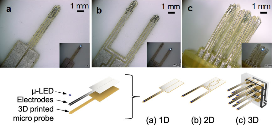
"In order to directly emit light into brain cells, the probe needed to be created from a thin material that was more flexible than silicon and that would not cause damage. Generally, this would be created in a cleanroom at a semiconductor factory, but the professor wanted me to create it in the lab with a 3D printer. At first, I was instructed to create electrodes for the μLED by cutting and attaching aluminum foil. I thought this would be impossible, but I explored methods while using literature for reference. In the end, I printed a structure with grooves and turned it into a mold. I applied a silver paste and formed it with a blade to create the electrodes. Ultimately, I attached an μm-sized LED. This creation process was very simple."
At first, Kawakami was skeptical about creating with a 3D printer, but it turned out to be a simple and inexpensive process. The shape and size can be freely adjusted, and she became confident that this would be useful for on-site medical research in developing countries.
"At the start of my study abroad period, I had trouble speaking in English, and I was also the only girl in the lab. I felt a bit isolated, but as I produced results, I started to open up. I think my experience of making things on my own in KOSEN gave me confidence."
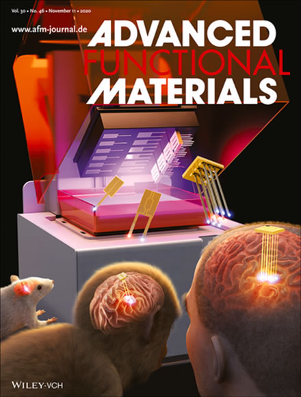
The results were published in "Advanced Functional Materials", an international, high-impact factor journal related to MEMS, and Kawakami was listed in the article as a key author of the paper. Also, a drawing of the probe designed by Kawakami was used on the cover of the journal.
She states, "I didn't think that I could achieve results like this as a graduate student. After graduation, I will work at Shimadzu to develop analytical machines and medical devices. I want to use my experiences from school to help me achieve my goal of developing medical devices." We look forward to her future activities.
Reference
Juhyun Lee, Kyle E. Parker, Chinatsu Kawakami, Jenny R. Kim, Raza Qazi, Junwoo Yea, Shun Zhang, Choong Yeon Kim, John Bilbily, Jianliang Xiao, Kyung‐In Jang, Jordan G. McCall, Jae‐Woong Jeong, “Optogenetic Probes: Rapidly Customizable, Scalable 3D‐Printed Wireless Optogenetic Probes for Versatile Applications in Neuroscience”, Advanced Function Materials 46/2020, 12 November 2020, https://doi.org/10.1002/adfm.202070305
Reporter's Note

Ms. Kawakami is the first student to appear in TUT Research Feature Story. The way she steadfastly pursued her dreams is an inspiration to us all. Aiming to become a world-class engineer, she joined the inaugural class of the Global Technology Architects Course (GAC) , established by Toyohashi University of Technology as a part of the Top Global University Project. She gained useful experiences along the way by living with international students on campus in Global House (a shared apartment style of student accomodation) and through studying abroad. Beyond language skills, she acquired the abilities required to be an internationally-minded person.
Additionally, she worked part time at a special nursing home for the elderly while she was a student. Based on her experience of living at home with a grandmother who required care, she keenly understands the need for very early diagnosis of Alzheimer's. We hope that she uses her characteristic persistence to achieve results for the development of medical devices. We're rooting for her future successes!
工夫を重ね、課題を克服してMEMSの世界に革新を
2021年3月に、豊橋技術科学大学の博士前期課程を修了した川上千夏さん。高専在学中から、将来は医療機器開発に携わりたいと、その要となるMEMS(Micro Electro Mechanical Systems)の研究を志した。豊橋技術科学大学に進学後は、澤田和明教授の研究室に所属して、イオンイメージセンサの開発に携わり、課題だったイオンの拡散を抑制する構造体の製作方法を開発したほか、留学先の韓国・KAISTでは、オプトジェネティクス(光遺伝工学)に用いるマイクロメータ(μm)サイズのLEDプローブを3Dプリンターで製作することに成功。成果の陰には、創意工夫を重ね、真摯に研究に取り組む川上さんの姿があった。
イオンの拡散を抑制する構造体に取り組む
イオンイメージセンサとは、集積回路技術とセンサ技術を融合させ、イオンの分布や動きをダイレクトに画像として捉えるバイオセンサである。センサに酵素膜をつけ、酵素反応により検出されるイオンを計測することで、間接的に神経伝達物質を画像化できることから、脳科学の進展や病気の早期診断などに役立つ画期的なセンサとして、医療分野を中心に大きな期待が寄せられている。
豊橋技術科学大学は、イオンイメージセンサの開発者である澤田和明教授を中心に研究が進められていて、すでにマウスの海馬スライスから放出される複数の神経伝達物質の可視化に成功。現在、産学連携により、実用化に向けた取り組みを加速しているところだ。
このイオンイメージセンサの課題となってきたのが、イオンの拡散である。澤田教授のもと、センサの構造体の製作に従事してきた川上千夏さんは、その理由を次のように説明する。
「イオンの濃度を計測するためには溶液中で測る必要がありますが、溶液内でイオンが拡散してしまうため、局所的なイメージングができないことが問題でした。つまり、輪郭が曖昧なピンボケのような画像しか得られなかったのです。最近ようやく2μmピッチで1細胞レベルまで計測できるセンサが開発されたのですが、画素間の距離が近いのでイオンの拡散の影響が大きくなってしまいます。そこで、イオンの拡散を抑制する構造体の製作を手掛けました」
当初、澤田教授からのオーダーは、集積回路の製作に用いられるフォトフィソグラフィ技術を使って、2μmピッチ、深さ5μmの井戸型の構造体をつくることだった。センサ上に酵素膜を成膜し、その上に井戸型の構造体を形成することで、酵素反応で生じたイオンが井戸の中にとどまって横方向の拡散を防ぎ、高精細な画像が得られるというわけだ。
「ところが、フォトフィソグラフィでは、表面に井戸型のパターニングをすることはできても、光の回折などの影響を受けて、深さ方向に解像することができませんでした。また、少しでもアライメント(位置合わせ)がずれると、すべての画素に構造体がかぶって、構造体として破綻してしまいます。試行錯誤を繰り返す中で、フォトリソグラフィでは限界があると見切りをつけ、何かいい材料はないかと探し当てたのがポーラスアルミナ膜でした」
ポーラスアルミナ膜の採用で高精細なイメージングに成功
ポーラスアルミナ膜は、自己組織的にナノポア配列を形成する薄膜材料で、ポア径が180~400nmと小さい。また、この膜はバイオセンサに応用されていて、生体適合性のある材料である点も採用の決め手になった。
「これを構造体に圧着すれば、1画素状に穴がいくつも空いているので、アライメントが少しくらいずれても問題はありません。半導体の上に54 μ㎡の酵素膜を成膜し、これを露光してアセチルコリン(ACh)を分解する酵素膜を64μmピッチでパターニングし、その上からポーラスアルミナ膜を圧着して実験をしたところ、イオンの拡散が抑制され、高精細な画像を得ることができることがわかりました」と川上さんは説明する。
構造体なしのセンサにアセチルコリンを滴下したところ、酵素反応で生成されたイオンが拡散し、時間の経過とともにパターンが見えなくなったのに対し、構造体有りのセンサでは、四角く形成されたACh感応部とその周囲の水素イオン感応部のパターンが、時間経過後も保持されたのである。確認のため、電位プロットでACh感応部と水素イオン感応部の電位変化を調べたところ、構造体有りのセンサではACh感応部のみイオンが検出できていることがわかった。
「最終的には、16μmピッチの酵素膜でもイメージングに成功しました。1細胞の大きさは数μm~50μmくらいなので、1細胞から放出される神経伝達物質を複数種類、高精細に検出できる可能性を示すことができました」
今後、澤田研では、アルミナ膜の最適な膜厚を検討するとともに、企業や研究機関との共同研究などによる動物実験を通じて、検出できる神経伝達物質を増やしていくという。
3Dプリンターで極小のLEDプローブの製作に成功
実は川上さん、大学4年次は1年間にわたり構造体のプロセスを検討するもうまくいかず、ポーラスアルミナ膜に辿り着いたのは修士1年のときだった。その後はアルミナの圧着に苦労することになる。結果として、水溶性の感光性樹脂を接着層として噛ませることで、うまく密着させることに成功。さらに高解像度の画像の出力に成功したのは、研究助成の成果報告会の直前のことだった。
「このまま何の成果も出ないまま修士が終わったらどうしようかと。成果報告会の1カ月前に成果がほしいと澤田先生に言われて焦りましたが、結果として高評価を得ることができて安心しました」(川上さん)
その探究心と実行力は、学部4年から修士1年にかけて海外実務訓練で滞在した留学先の韓国・KAIST(Korea Advanced Institute of Science and Technology)でも大いに発揮された。光で脳細胞などの機能を制御する技術として注目されるオプトジェネティクス(光遺伝工学)の研究に従事し、わずか5カ月という短期間で、細胞に光を照射するためのμmサイズのLEDプローブ(μLED)の製作に成功したのだ。
「脳の細胞に直接挿して光を照射するため、ダメージを与えないよう、プローブはシリコンよりも柔らかく、薄い材料で作成する必要がありました。従来は半導体工場のクリーンルーム内で製作していましたが、これを研究室の3Dプリンターでつくってほしいというのが、教授からの要望でした。当初はアルミホイルを切り貼りし、μLED用の電極をつくるよう指示され、これでは絶対にできないと思い、文献を参考にしながら方法を探りました。結局、溝のある構造体をプリントして、これを鋳型のようにして、シルバーペーストを塗って、ブレードで成形して電極をつくり、最後にμmサイズのLEDをつけるというとてもシンプルな工程で製作しました」
当初は、3Dプリンターでつくることに懐疑的だったという川上さんだが、3Dプリンターなら、簡単なプロセスで安くつくれるうえ、形や大きさも自在に変えることができ、途上国などの医療研究の現場でも役立つと確信するようになった。
「留学したばかりの頃は、英語を話すのが苦痛で、研究室に女子が私一人だったこともあり、やや孤立していたのですが、成果を出すうちに打ち解けました。高専で自ら手を動かしてモノづくりをしてきた経験が生きたと思っています」
この成果は、高いインパクトファクターで知られるMEMS関係の国際ジャーナル『Advanced Functional Materials』に掲載され、川上さんも主要メンバーとして論文に名を連ねた。さらに、ジャーナルの表紙に、このプローブをあしらった川上さんのデザイン画も採用された。
「まさか、修士でこれだけの成果を出すことができるとは思いませんでした。卒業後は分析装置や医療機器の開発を手がける島津製作所に就職しますが、在学中に得たさまざまな経験を糧に、目標としてきた医療機器開発に携わっていきたいと思っています」と、川上さん。今後のさらなる活躍に期待したい。
(取材・文=田井中麻都佳)
取材後記
TUT ResearchのFeature Storyに学生としては初登場となる川上さん。夢に向かって着実に進んでいく姿が実に頼もしかった。世界で活躍する技術者をめざして、豊橋技術科学大学のスーパーグローバル大学プロジェクトで新設されたグローバル技術科学アーキテクト養成コース(GAC)の第1期生として入学。キャンパス内のシェアハウス型学生宿舎グローバルハウスでの留学生たちとの共同生活や留学を通じて経験を積み、語学だけでなく国際人として必要なリテラシーも身につけた。さらに、在学中は特別養護老人ホームでアルバイトもした。かつて介護の必要な祖母と実家で暮らした経験から、アルツハイマーの超早期診断の必要性を強く感じているという。ぜひとも、そうした医療機器開発の場で持ち前の粘り強さを発揮して、成果を出してもらいたい。応援しています!
Researcher Profile
Chinatsu Kawakami
Chinatsu Kawakami graduated from National Institute of Technology (KOSEN), Anan College, before joining the Global Technology Architects Course (GAC) at TUT. Having completed her masters degree, she started working at Shimadzu Corporation in April 2021. In her time as a student at TUT, she received multiple awards:
-
Best Poster Presentation Award, The 36th Symposium on Sensors, Micromachines and Applied Systems (November 21, 2019)
-
Best Presentaion Award, TUT 2020 Master’s degree thesis review (February 19, 2021)
-
TUT Top Global Leader Award (March 23, 2021)
Reporter Profile

Madoka Tainaka is a freelance editor, writer and interpreter. She graduated in Law from Chuo University, Japan. She served as a chief editor of "Nature Interface" magazine, a committee for the promotion of Information and Science Technology at MEXT (Ministry of Education, Culture, Sports, Science and Technology).
ここでコンテンツ終わりです。