
ここからコンテンツです。
Affordable multiferroic material
An important first step towards a wide-range of practical applications of advanced materials By Go Kawamura
An international research team led by Toyohashi University of Technology, with the collaboration of the Japan Fine Ceramics Center, the National Institute of Technology Ibaraki College, the International Iberian nanotechnology Laboratory, Chang’an university and The University of Erlangen-Nuremberg, has developed a novel liquid process for fabrication of an affordable multiferroic nanocomposite film. The multiferroic material obtained by the novel process has a strong correlation between its electric and the magnetic properties which makes it a promising material for various future applications such as low-power-consumption large-volume memory, spatial light modulators and unique sensors, etc.
Multiferroic materials combine electrical (ferroelectric) and magnetic (ferromagnetic) properties and have a strong correlation between these properties, i.e. they exhibit a magnetoelectric effect. Their development is expected to realize more versatile and higher performance next-generation electrical and magnetic devices. In recent years, several methods of production of multiferroic films exhibiting large magnetoelectric properties have been reported. However, these processes require large and extraordinarily expensive vacuum devices, making them impractical for fabricating materials with a large surface area in particular. As a result, multiferroic materials have only been used in a very limited range of applications.
The new material with advanced multiferroic properties developed by the research team, however, was created by combining several liquid-phase methods that are relatively inexpensive and simple.
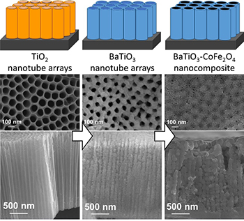
The lead author, Associate Professor Go Kawamura of Toyohashi University of Technology explained, "In order to fabricate a material that exhibits advanced multiferroic properties, it is necessary to combine ferroelectric and ferromagnetic materials appropriately and periodically on the nanometer scale. In the past, nanopillar array structures were fabricated in a self-organized manner using gas-phase methods, and a large magnetoelectric effect was observed in such materials. However, the gas-phase methods required the use of large and expensive equipment, and it was practically impossible to increase the area of the sample. Therefore, we worked on the fabrication of nanopillar array-like composite films using only affordable and simple liquid-phase methods. We were able to demonstrate that the multiferroic composite film we created has a local epitaxial relationship at the interface between the ferroelectric and the ferromagnetic materials, thereby producing a large magnetoelectric effect. Compared to conventional gas-phase processes, multiferroic composite films can be produced at a much lower cost and can be used for larger areas."
This study required an interdisciplinary approach since it required expertise across a variety of specialties. Therefore, the research team collaborated with specialists in dielectric materials and magnetic materials, specialists in observation of nanostructures using electron microscopes, and specialists in liquid-phase synthesis, among others, from various institutions in Japan and overseas. The novel process was developed by combining these advanced specialties.
The research team believes that greater precision in the creation of controlled nanostructures can lead to a further improvement of the magnetoelectric effect, and will continue to optimize the process. Ultimately, the team plans to produce large area materials, which is also a feature of the process that was developed, and apply them to a spatial light modulator to develop applications such as spatial displays that can build huge three-dimensional images.
This work was financially supported by the Program for Fostering Globally Talented Researchers (R2802), JSPS. TG, YN, and MI acknowledge JSPS KAKENHI [Grant Nos. 17K19029, 16H04329, and 26220902]. TG acknowledges JST PRESTO [Grant No. JPMJPR1524]. FLD acknowledges the N2020; Nanotechnology based functional solutions (NORTE-45-2015-02).
Reference
Go Kawamura, Kentaro Oura, Wai Kian Tan, Taichi Goto, Yuichi Nakamura, Daisaku Yokoe, Francis Leonard Deepak, Khalil El Hajraoui, Xing Wei, Mitsuteru Inoue, Hiroyuki Muto, Kazuhiro Yamaguchi, Aldo R. Boccaccini and Atsunori Matsuda (2019). Nanotube array-based barium titanate–cobalt ferrite composite film for affordable magnetoelectric multiferroics. Journal of Materials Chemistry C, 7, 10066-10072. DOI: 10.1039/C9TC02442E
http://dx.doi.org/10.1039/C9TC02442E
マルチフェロイック材料を安価・簡便に作る
最先端材料の汎用化に向けた第一歩By 河村 剛
豊橋技術科学大学は、(一般財団法人)ファインセラミックスセンター、茨城工業高等専門学校、ポルトガルの国際イベリアナノテクノロジー研究所、中国の長安大学、ドイツのエアランゲン-ニュルンベルグ大学との共同研究により、高度なマルチフェロイック特性を示すナノ複合膜を、安価で簡便に作製できる液相プロセスを開発しました。このプロセスで得られるマルチフェロイック材料は、電気的特性と磁気的特性の間に強い相関をもつため、将来的に低消費電力・大容量のメモリデバイスや空間光変調器、様々なセンサ等への応用が期待されます。
電気的な特性(強誘電性)と磁気的な特性(強磁性)を併せもち、かつそれらの特性間に強い相関をもつ(電気磁気効果を示す)マルチフェロイック材料は、より多機能で高性能な次世代電気・磁気デバイスの実現に向けて開発が期待されています。近年、大きな電気磁気特性を示すマルチフェロイック膜の作製例がいくつか報告されましたが、それらのプロセスでは、非常に大型で高額な真空装置などが必要であり、特に大面積の材料を作製することは現実的ではありませんでした。そのため、マルチフェロイック材料の応用検討はごく限られた範囲に限定されていました。
そこで、研究チームは比較的安価で簡便ないくつかの液相法を組み合わせることで、高度なマルチフェロイック特性を示す材料を作製するプロセスを開発しました。
「高度なマルチフェロイック特性を示す材料を作製するには、強誘電体と強磁性体をナノメートルスケールで適切にかつ周期的に複合化する必要があります。従来は、気相法によって、自己組織的にナノピラーアレイ構造などを作製し、その材料において大きな電気磁気効果が観測されていました。しかし、採用されていた気相法では、大型で高価な設備の使用が必須であり、また試料の大面積化が現実的に不可能でした。そこで、安価で簡便な液相法のみを駆使してナノピラーアレイライクな複合膜の作製に取り組みました。
今回開発したプロセスで得られるマルチフェロイック複合膜では、強誘電体と強磁性体の界面において、局所的にエピタキシャルな関係を有していることが明らかとなり、それによって大きな電気磁気効果を発現することがわかりました。従来の気相プロセスに比べて非常に安価にマルチフェロイック複合膜を作製することができ、かつ大面積化にも対応可能です。」と筆頭著者である豊橋技術科学大学の河村剛准教授は説明します。
この研究は、様々な専門性を必要とする学際的なものでした。そこで、国内外の様々な機関に在籍している誘電材料や磁性材料の専門家、電子顕微鏡でのナノ構造観察の専門家、液相合成法の専門家などと協力し、それぞれの高度な専門性を融合することで、これまでにないプロセスの開発につながりました。
研究チームは、制御されたナノ構造をより精密に作り込むことで、電気磁気効果をさらに改善できると考えており、引き続きプロセスの最適化に取り組んでいます。最終的には、開発したプロセスの特徴でもある材料の大面積化を行い、空間光変調器へ応用することで、巨大な3次元像を構築できる空間ディスプレイなどへの展開を考えています。
Researcher Profile

| Name | Go Kawamura |
|---|---|
| Affiliation | Department of Electrical and Electronic Information Engineering |
| Title | Associate Professor |
| Fields of Research | Nanomaterials Science |
ここでコンテンツ終わりです。