
ここからコンテンツです。
Professional in research and development of new materials through transmission electron microscopy (TEM)
Hiromi Nakano
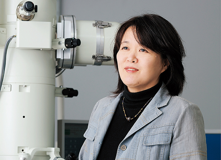
Professor Hiromi Nakano has been observing and analyzing materials by transmission electron microscopy (TEM) for many years at companies and universities. She is a TEM professional who is now attracting attention from domestic and foreign researchers and enterprises for her tenacious efforts in areas such as discovering unknown material properties and developing new materials with controlled crystal structure and texture at the atomic level. Recently, she succeeded in developing innovative new oxide phosphors used for white LEDs together with students in her lab. We talked with her about the contents of her research and the beliefs that guide it.
Interview and report by Madoka Tainaka
Tenacity is indispensable for TEM observations
"My specialty is to do material analysis using a transmission electron microscope (TEM)," Professor Hiromi Nakano says.
A TEM is an electron microscope that irradiates an observation specimen with an electron beam and searches the microstructure of the surface or interior of the observation object with the transmitted electron beam. With TEM, it is possible to analyze the texture and crystal structure of materials at the atomic level, and the technique is widely used for analyzing everything from inorganic materials such as ceramics and metals to organic materials and biomaterials. TEM is useful for material property control and new material design, and is an indispensable device for nanotechnology development. It is also used in various fields such as materials engineering, biology and medicine because researchers can observe samples while heating or cooling them, making it possible to capture images of shape change and behavior of nanoparticles due to temperature change.
"However, you must be very persistent to make observations with TEM. To be able to transmit the electron beam, the thickness of the sample must be 0.1 μm or less with a diameter within 3 mm. To achieve this one punctures the center of the sample with an argon ion beam, but if it is a thin laminated material, important parts may be peeled apart in the course of fabricating the thin film samples. If this happens one must start over again from the beginning. With difficult samples, it sometimes takes more than two months to make one thin film sample," says Nakano.
Nakano was once requested to observe aluminum nitride, which has the world's highest level of high thermal conductivity, by TEM. The material was produced by adding yttrium oxide to aluminum nitride as a sintering aid and applying heat treatment in a reducing atmosphere. Its high thermal conductivity was believed to be a result of the loss of the grain-boundary phase from that process. However, Professor Nakano was able to demonstrate with TEM photography that the grain-boundary phase remained even after heat treatment for 100 hours.
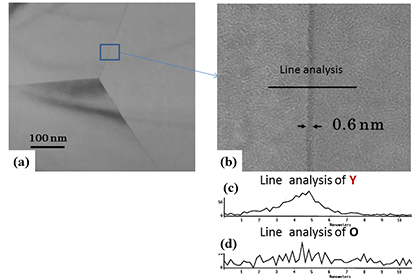
"When I presented a TEM image showing a thin layer containing 0.6 nm of yttrium including at the grain boundary at a conference, the place erupted. I was an unknown researcher at that time, and researchers didn’t believe me even though I showed them the TEM picture as evidence. The researchers who were present exclaimed, ‘We have taken images many times, but could not observe the grain-boundary phase, so why is it only you that found it?’ I replied, ‘It’s perseverance.’ After that, I became called ‘The person with perseverance’ for a while," says Nakano, laughing.
It was an accomplishment that was achieved as a result of Professor Nakano’s observation technique that makes grain boundaries precisely vertical to the electron beam. To that extent, Nakano says that TEM research requires a certain amount of skill and tenacity, and, above all, beliefs which are firmly rooted in theory.
Development of phosphor materials started from an educational viewpoint
However, Nakano also feels that it is difficult for students with a limited research period to be forced to only do TEM research. "Especially recently, there is a strong tendency to seek results as soon as possible," says Nakano. Therefore, in recent years, she has been working in the laboratory on the development of oxide phosphor materials used in white LEDs.
For white LEDs used in applications such as lighting and LCD monitors, methods such as combining yellow phosphor on a blue LED chip or combining red, green and blue phosphors on a near ultraviolet LED chip are used. While the former has the merit that it can be realized at a low cost, there is the demerit that the combination of only blue and yellow has poor color rendering properties and only a cold white can be reproduced.
"For this reason, I started thinking about red oxide phosphor. It can be sintered at a lower temperature than nitride phosphor that is currently used at normal pressure, and because it is an oxide, it is highly stable, and is also easy to procure. It is also non-toxic, of course." Specifically, red phosphor is prepared with a Li-Ta-Ti-O system solid solution as a matrix then adding a rare earth or the like as an activator.
"The students are more motivated because we can confirm light emission only by shining light on a sample with phosphor. Of course, it is difficult to find good synthesis conditions, and there may be repeated failures, but in fact, there is no such thing as a failure. Sometimes, unexpected results are born from failure. Our mission as researchers is to derive mechanisms from there. I hope that as many students as possible can experience this real pleasure."
In January 2016, Nakano Laboratory succeeded in developing a superior material with internal quantum efficiency (the rate at which absorbed energy is converted to light) of 98% in phosphors with trivalent europium ions as luminescent center ions. This new technology was announced in the Nikkan Kogyo Shimbun. However, since the external quantum efficiency is about 40%, there is room for improvement, and Nakano plans to develop phosphor materials other than red while working in cooperation with companies for practical applications.
Aiming for research with originality
On the other hand, Professor Nakano continues to conduct research based on TEM concurrently. Recently, she presented the results of over four and a half years of research at an international conference as an invited speaker and summarized them in a paper.
"When making a polycrystalline oxide, if a very strong magnetic field is applied, the particles become oriented in a certain direction, and a relatively large bulk material like a single crystal can be made. As a result, I was able to create a material with high anisotropy in the high electrical property called the Qf value. I went to Austria and discussed why this occurs with a famous Indian researcher who is the expert on that topic, but I still did not understand the answer, so I was convinced that this must be a mechanism unique to this material."
Actually, this material, an oxide derived from titanium, is a unique material that forms a singular periodic structure called an M-phase in a certain composition area, in the same way as phosphor. It took time and perseverance to synthesize and analyze the material, but results were achieved thanks to the tenacity of Professor Nakano.
By the way, Professor Nakano recently learned that the "M" of M-Phase is named after the female researcher Maria who first discovered this phase. They happened to meet two years ago at an international conference, and Nakano says that she was able to solve a long-standing puzzle. International conferences are important opportunities to meet world famous researchers and speak directly to them.
Professor Nakano says, "It is only meaningful to do research with high originality that no one has ever done before." Thanks to her indomitable perseverance, she is being heralded as a role model for female researchers everywhere.
Reporter's Note
Professor Nakano was born and raised in Sabae City, Fukui Prefecture, known as the city of glasses, and comes from a family of glasses’ frame makers. She says that she was a born engineer from an early age who became familiar with machines and tools such as ultrasonic cleaners and drilling machines in the workshop.
"I thought that life with its ups and downs was compelling as I watched my father, who was a designer and manufacturer of glasses frames." After graduating from graduate school, she started to work at Murata Manufacturing Co., Ltd. where she was the first female to pass the promotion exam for a management career. However she left at the age of 29 and joined Ryukoku University. At 33, she married and had a child, after which she devoted herself to research without rest, returning to her alma mater, Toyohashi University of Technology, at the age of 50. Nakano has lived a varied life as a researcher.
"I was writing papers while raising my child, and there were times when it was hard, but I have survived through perseverance," she laughs. That smile was full of the pride and brightness peculiar to someone who has braved the stormy seas.
透過型電子顕微鏡(TEM)のプロとして、新材料の研究開発を究める
企業および大学において、長年にわたり、透過型電子顕微鏡(TEM)による材料の観察・解析を行ってきた中野裕美教授。粘り強い取り組みで、未知の材料特性を発見したり、原子レベルで構造・組織を制御した新材料を開発したりするなど、いまや国内外の研究者や企業から注目を集めるTEMのプロフェッショナルである。最近では、学生とともに白色LEDに用いられる酸化物蛍光体において、画期的な新材料の開発に成功した。その研究内容と研究者としての信念を聞く。
TEMによる研究には粘り強さが不可欠
「私の専門は、透過型電子顕微鏡(TEM)を使って材料解析をすることです」と語る中野裕美教授。
TEMとは、観察対象に電子線を照射し、透過した電子線により、観察対象の表面や内部の微細構造を探る電子顕微鏡である。TEMでは原子レベルでの組織・構造解析が可能で、セラミックスや金属といった無機材料から有機材料、生体材料までと幅広く利用され、材料の物性制御や新素材設計に役立てられるなど、ナノテクノロジーの進展に欠かせない装置だ。試料を加熱、あるいは冷却しながら観察し、温度変化によるナノ粒子の形状変化や挙動などを撮像することもできるため、材料工学をはじめ、生物学や医学など、さまざまな分野で活用されている。
「ただ、TEMによる観察というのはとても根気がいるんです。電子線を透過させるために、試料の厚みは0.1 μm以下で、直径3 mm以内の薄片にする必要があります。そのため、中心部にアルゴンのイオンビームで穴を開けていくのですが、薄く積層している材料だと、薄片試料作製の過程で大事な箇所がぽろっと剥がれてしまうことがある。そうすると、また一からやり直しです。難しい試料の場合には、一つの薄片試料を作製するのに2カ月以上かかることもありました」と中野教授は語る。
かつて中野教授は、世界最高レベルの高熱伝導率を有する窒化アルミニウムの材料を、依頼されてTEMで観察したことがあった。その窒化アルミニウムは、緻密化と熱伝導率を向上させるため、焼結助剤として酸化イットリウムを添加した材料で、還元雰囲気下で熱処理をすることにより、粒界相は消失し、それによって熱伝導率が高まると考えられてきた。ところが、中野教授は、100時間熱処理しても、粒界相は残存するという、証拠のTEM写真の撮像に成功したのだ。
「学会で、粒界に残る0.6 nmのイットリウムを含む薄い層が写ったTEM写真を発表したら、その場が騒然としたんです。当時はまだ無名だったこともあり、証拠のデータを見せてもなかなか信じてもらえず、居合わせた研究者から、『僕たちは何度も撮影したが、粒界相は見えなかった。なぜ、あなたにだけ見えるんですか?』と詰め寄られたほど。思わず、『根性で観察したんですよ』と言い返したら、その後しばらく、“根性の人”と呼ばれる羽目になりました」と笑う。
それは、粒界を電子線に対して正確に垂直に立てる観察技術を持つ中野教授だからこそ成し遂げた快挙だった。それほどに、TEMを用いた研究には、確かなスキルと粘り強さ、そしてなによりも理論に基づく信念が必要なのだという。
教育的な観点から蛍光体材料の開発へ
しかし、研究期間が限られる学生にTEMの研究だけを強いるのは難しいとも感じている。「とくに最近は、結果を早く求める傾向が強い」と中野教授は言う。そこで研究室では、近年、白色LEDで使われる酸化物蛍光体の開発を手がけている。
照明や液晶モニターなどに採用される白色LEDには、青色のLEDチップに黄色の蛍光体を組み合わせたり、近紫外のLEDチップに赤・緑・青の蛍光体を組み合わせたりする方法などがあるが、前者は廉価に実現できるというメリットがある一方で、青と黄色の組み合わせだけでは演色性に乏しく、寒々しい白色しか再現できないというデメリットがある。
「そうしたことから目をつけたのが赤色の酸化物蛍光体です。現在、実用化されている窒化物蛍光体に比べて低い温度かつ常圧で焼成でき、酸化物なので安定性も高く、材料も手に入れやすいのが特長です。もちろん毒性もありません」具体的には、Li-Ta-Ti-O系の固溶体を母体とし、これに希土類などを賦活材として添加して赤色蛍光体をつくる。
「蛍光体というのは、光を当てただけで発光を確認できるので、学生たちの目の色が変わるんですね。もちろん、なかなかいい合成条件が見出せず、失敗が続くこともありますが、本当は失敗なんて一つもない。ときには、失敗から思いがけない成果が生まれることもあります。そこからメカニズムを導き出すのが、我々、研究者の使命。その醍醐味を一人でも多くの学生にも経験してほしいですね」
2016年1月、中野研究室では、3価のユウロピウムイオンを発光中心イオンとする蛍光体において、内部量子効率(吸収したエネルギーが光に変わる率)98%という、すぐれた材料の開発に成功し、日刊工業新聞にその新技術が掲載された。ただ、外部量子効率は40%程度と改良の余地があることから、今後は実用の用途に合わせ、企業と連携しながら、赤色以外の蛍光体材料開発にも取り組んでいく予定だ。
オリジナリティのある研究をめざして
一方で、中野教授は、TEMを基盤とした研究も並行して続けている。最近、4年半越しの研究成果を国際会議の招待講演で発表し、論文にまとめている。
「多結晶の酸化物をつくる際に、非常に強い磁場をかけると、粒子が一定の方向に配向し、比較的大きい、まるで単結晶のようなバルク体が作製できます。その結果、Qf値と呼ばれる電気特性の高い異方性を有する材料を創製することができたのです。なぜそうなるのか、オーストリアまで赴き、その道の専門家であるインド人の著名な研究者と議論したのですが、それでも答えがわからなかった。そのとき、これはこの材料特有のメカニズムに違いないと確信したのです」
実は、この材料も先の蛍光体と同じく、チタン由来の酸化物で、ある組成域でM-相と呼ばれる、特異な周期構造を形成するユニークな材料である。その合成と解析には、時間と根気がかかったが、それを中野教授の持ち前の粘り強さで成し遂げたことで成果に導いた。
ちなみに、M-相の“M”は、この相を最初に発見した女性研究者のマリアという人の名にちなむことを、中野教授は最近になって知った。一昨年、国際会議で偶然の出会いがあり、本人からそのことを告げられ長年の疑問が解けたという。国際会議は、世界の著名な研究者と出会い、直接話せる大事な機会の場でもあるのだ。
「まだ誰も手をつけたことがない、オリジナリティの高い研究を手がけることにこそ、意味がある」と語る中野教授。根気強く挑戦を続ける中野教授の姿はいま、女性研究者のロールモデルとしても注目を浴びている。
(取材・文=田井中麻都佳)
取材後記
中野教授は、メガネの街として知られる福井県鯖江市で、メガネフレームの制作をする家に生まれ育った。幼い頃から、仕事場にある超音波洗浄機やボール盤などの機械や工具に慣れ親しんできた、生まれながらの「工学屋」だと自身を語る。
「メガネフレームのメーカーでもあり、デザインも手がけていた父親の背中を見ながら、浮き沈みのある人生も面白いなと思っていました」という言葉通り、大学院修了後は、村田製作所に務め、女性初の総合職として昇格試験にも合格したが、29歳で退職し、龍谷大学へ。33歳で結婚して一児を授かり、その後も休むことなく研究に専念し、50歳のとき母校である豊橋技科大に赴任。変化に富む研究者人生を歩んできた。
「子育てをしながら論文を書き、大変なときもありましたけど、それこそ根性で乗り切ってきました」と笑う。その笑顔は、荒波を乗り越えてきた人特有の自負と明るさに溢れていた。
Researcher Profile
Dr. Hiromi Nakano
Dr. Hiromi Nakano received her B.S., M.S., and Dr. (Eng.) from Toyohashi University of Technology, Japan in 1981, 1983 and 2000, respectively. She joined Murata Manufacturing Co., Ltd. in 1983 then transferred to Ryukoku University in 1989. She joined the Cooperative Research Facility Center in Toyohashi University of Technology as an associate professor in 2009 and presently works as a professor and presidential advisor (Gender Equality). Her current interest is in the synthesis of new phosphors and characterization of ceramic materials using a transmission electron microscope to control of the material properties and the design of new materials. - See more at: http://www.crfc.tut.ac.jp/nakano/index.html
Reporter Profile
Madoka Tainaka is a freelance editor, writer and interpreter. She graduated in Law from Chuo University, Japan. She served as a chief editor of “Nature Interface” magazine, a committee for the promotion of Information and Science Technology at MEXT (Ministry of Education, Culture, Sports, Science and Technology).
ここでコンテンツ終わりです。