
ここからコンテンツです。
Wirelessly Supplying Power to Brain
Implantable device composed of a flexible antenna and silicon large-scale integration chips By Ippei Akita
Ippei Akita and his colleagues have developed a technique to implement silicon large-scale integration chips in a very thin (10 μm) film. This fabrication method has the potential to realize a low-invasive flexible device for monitoring brain activity. This study will contribute to the development of brain-machine interface systems.
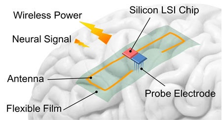
Human and animal movements generate slight neural signals from their brain cells. These signals obtained using a neural interface are essential for realizing brain-machine interfaces (BMI). Such neural recording systems using wires to connect the implanted device to an external device can cause infections through the opening in the skull. One method of solving this issue is to develop a wireless neural interface that is fully implantable on the brain.
However, the neural interface implanted on the brain surface should be of small size and minimally invasive. Furthermore, it requires the integration of a power source, antenna for wireless communication, and many functional circuits.
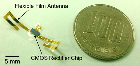
Now, Ippei Akita and his colleagues have developed a wafer-level packaging technique to integrate a silicon large-scale integration (LSI) chip in a very thin (10 μm) film. Using flip-chip bonding, the researchers have managed to fabricate a Wireless Power Transmission (WPT) device including a flexible antenna and rectifier chip.
The first author PhD candidate Kenji Okabe said, “We have investigated how to integrate flexible antenna and high-performance circuits and tried this fabrication method with process conditions obtained through experiments." Assistant Professor Ippei Akita, who is leading the project, said, “Using flexible device technology is a good solution to implement bio-compatible passive devices such as antennas or sensor electrodes. On the other hand, silicon-based integrated circuit technology, which has long history, is suitable for ultra-low-power systems with many functionalities. So, we believe that combining these technologies is essential to establish such minimum invasive implantable devices.”
The fabricated device is of size 27 mm × 5 mm, and 97% of the device area is composed of a flexible film as the silicon chip has a small area. Therefore, it has sufficient flexibility to fit the shape of the brain surface. In addition, the researchers achieved WPT to the device immersed in saline.
This WPT device can supply electricity to other circuits included in the neural interface.
The researchers are trying to integrate more functions (e.g., amplifiers, analog-to-digital converters, signal processors, and radio frequency circuits) to an LSI chip. This study may contribute to the development of safer BMI systems.
This work is partially supported by Grants-in-Aid for Scientific Research (A) #25249047, Young Scientists (A) #15H05525, and (B) #25820141 from the Japan Society for the Promotion of Science.
Reference
Kenji Okabe, Horagodage Prabhath Jeewan, Shota Yamagiwa, Takeshi Kawano, Makoto Ishida, and Ippei Akita (2015). Co-design method and wafer-level packaging technique of thin-film flexible antenna and silicon CMOS rectifier chips for wireless-powered neural interface systems, Sensors, Article first published online: 16 Dec., 15(12), 31821-32. DOI: 10.3390/s151229885.
脳に電力を送る
フィルムとシリコンチップの一体化によるフレキシブルな埋め込みデバイス秋田一平助教らは、神経インターフェイスの開発に向けて、フィルムデバイスにシリコン基板による回路チップを実装する手法を開発しました。厚さ10μmのフィルムアンテナに小型の整流器を集積することで、脳表面に張り付けられる柔軟さを持った、無線電力伝送デバイスを実現しました。この実装手法は、脳機能を解明するための無線神経インターフェイスの開発に貢献します。
ヒトや動物は、手足を動かした際に、脳の神経細胞から微弱な神経電位を生じます。この神経電位の解析は、ヒトとロボットを繋ぐブレインマシンインターフェイス(BMI:Brain Machine Interface)の実現に向けて盛んに研究されています。現在、ワイヤを用いて脳表面に埋め込まれた電極から神経電位の計測が行われていますが、頭蓋骨の開口部から感染症を引き起こす懸念があります。そのため、長期間にわたって脳の信号を観測するために、生体内に完全に埋め込む無線神経インターフェイスの開発が要求されています。
しかし、頭部へ埋め込む神経インターフェイスは、埋め込む際に生体にダメージを与えないために、小型かつ低侵襲でなければなりません。また、増幅器や信号処理等の高機能な回路と、通信をするためのアンテナ、さらにデバイスを駆動する電源が必要になります。
秋田一平助教らの研究チームは、半導体デバイスのパッケージ技術を用いて、シリコン基板による高機能かつ小型な回路チップを、厚さ10μmのフレキシブルフィルムに実装する手法を開発しました。研究者らは、無線神経インターフェイスに電力を伝送するために、提案した製作手法を用いて、整流器チップとフィルムアンテナを一体化した無線電力伝送デバイスを製作しました。
「我々は、無線電力伝送デバイスを実現するために、如何にして高効率なアンテナを実現し、回路機能を集積するかを検討した。そして、今回、薄膜かつ大面積のフィルムアンテナに対して、シリコン基板で製作した回路チップを実装する手法に挑戦した。」と、第一著者の岡部は述べています。
また、本プロジェクトを先導する秋田助教によると、「近年盛んに研究が行われているフレキシブルデバイス技術は、アンテナやセンサ・電極などの実現に非常に有用である。一方で、長い歴史を持つシリコン集積回路技術は、低消費電力・高機能なシステムを実現できるため、それぞれの技術が得意とする領域を適切に融合させることで、最適なシステムを実現することができると考えている」と方向性の意義について述べています。
製作されたフレキシブルデバイスは、5mm×27mmの面積であり、シリコン基板による回路面積は全体の3%を占めています。そのため、本デバイスは、大部分がフレキシブルフィルムで構成されており、脳の形状に対して柔軟に密着します。また、製作したデバイスを水槽に浸して、10cmの距離で無線電力を伝送することに成功しました。
埋め込みデバイスに無線電力を供給する事により、様々な回路を駆動する事が可能になります。研究者らは、今後、シリコンチップに更なる回路機能を搭載し、無線で脳の信号を取り出す事を目指しています。無線神経インターフェイスは、ヒトに不自由の無い義肢を提供するBMIシステムの構築に貢献します。
本研究は、文部科学省・日本学術振興会科研費・基盤研究(A)25249047、若手研究(A)15H05525並びに若手研究(B)25820141の支援を受けて遂行されました。
Researcher Profile

| Name | Ippei Akita |
|---|---|
| Affiliation | Department of Electrical and Electronic Information Engineering |
| Title | Assistant Professor |
| Fields of Research | Analog signal processing / Electronic circuits / Integrated circuits |
ここでコンテンツ終わりです。