
Research highlights
Optoelectronic integrated circuits: Silicon and nitride LEDs integrated onto a single chip for one-bit digital counters
Silicon-based semiconductor devices dominate the microelectronics industry and are used for the fabrication of high density integrated circuits comprising of memory and processing devices. However, silicon has an indirect band gap, which severely limits its use for fabricating photonic devices such as light emitting diodes (LEDs) and lasers. A innovative solution to this problem would be the integration of silicon devices with LEDs produced using direct band gap compound semiconductors, in the form of optoelectronic integrated circuits (OEICs).
Here, Akihiro Wakahara and colleagues at Toyohashi University of Technology (Toyohashi Tech) demonstrate the first realization of a one-bit counter circuit OEIC with an optical output consisting of silicon field effect transistors integrated with gallium phosphide nitride (GaPN) LEDs on a single chip.
The monolithic integrated circuits were fabricated using lattice matched Si/GaPN/Si heterostructures grown on silicon substrates in a dual chamber molecular beam epitaxy (MBE) system. Notably, growth of the silicon capping layer at a high temperature of 850℃ led to a dramatic reduction of the threshold voltage to -2.1 V and an increase of the channel mobility of the p-MOSFET to 82 cm2Vs. This improvement is attributed to a decrease in phosphorus incorporation during the growth of the capping layer.
The one-bit counter circuit fabricated using the n-Si/p-GaPN/n-GaPN/GaP/n-Si heterostructure exhibited normal operation, where red light emission from the input and output indicators was in synchronization with the input and output logical voltages.
- Reference
- K.Yamane1, K. Noguchi1, S. Tanaka1, Y. Furukawa1, H. Okada2, H. Yonezu1, and A. Wakahara1,2
- Operation of Monolithically-Integrated Digital Circuits with Light Emitting Diodes Fabricated in Lattice-Matched Si/III–V–N/Si Heterostructure
- Applied Physics Express 3, 074201, (2010)
- Abstract and restricted links: http://apex.jsap.jp/link?APEX/3/074201/
- DOI: 10.1143/APEX.3.074201
- 1Department of Electrical and Electronic Information Engineering, Toyohashi University of Technology, Toyohashi, Aichi 441-8580, Japan
- 2Intelligent Sensing System Research Center, Toyohashi University of Technology, Toyohashi, Aichi 441-8580, Japan
- Related information
- Frontiers of Intelligent Sensing:http://www.gcoe.tut.ac.jp/english/gaiyou/index4.html

Akihiro Wakahara
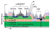
One-bit counter consisting of a p-MOSFET and GaPN light emitting diode
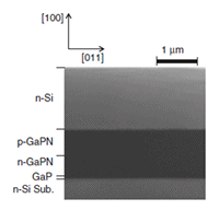
Transmission electron microscope image showing the n-Si/p-GaPN/n-GaPN/GaP/Si heterostructure.
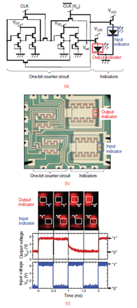
(a) Circuit diagram of the one-bit counter; (b) Optical image of an actual circuit; (c) Synchronization of the LED emission with input and output circuit voltages