
Research highlights
Inorganic-Organic Hybrid Photovoltaic Devices as sustainable energy generation
Hybrid inorganic-organic photovoltaic devices are attractive as next generation high efficiency thin film solar cells, but the photovoltaic performance is still low level compared with inorganic solar cells of Si, Cu(InGa)Se2 , and organic solar cells of C60.
With this background it is necessary to investigate the fundamental aspects of these materials including the molecular configuration, energy state, and band alignment to improve photovoltaic performance.
Here, Masanobu Izaki and colleagues fabricated hybrid p-Cu2O/C60 photovoltaic device on <111>-oriented Au -coated Si substrates by electro-deposition of Cu2O layer followed by vacuum evaporation of the C60 layers as an acceptor layer.
The C60 layers exhibited face centered cubic molecular configuration on the <111>-oriented Cu2O layer, and the preferred orientation changed from random to <111> plane depending on the preparation methods.
The electrical characteristics of hybrid photovoltaic devices varied depending on the C60 molecular configuration, and a rectification characteristic with an ideality factor of approximately 1 was achieved for hybrid <111>-Cu2O/<111>-fcc- C60/ bath cuproine photovoltaic devices.
This research underscores the importance not only of the configuration of both organic and inorganic semiconductors but also of the introduction of nanostructures in the light-absorbing layer and optimization of the band alignment at the heterointerface in hybrid photovoltaic devices.
- Reference:
- Authors: Masanobu Izaki, Takamasa Saito, Tatsuya Ohata, Kazufumi Murata, Binti Mohamad Fariza, Junji Sasano, Tsutomu Shinagawa, Seiji Watase.
- Title of original paper: Hybrid Cu2O diode with orientation-controlled C60 polycrystal.
- Journal, volume, pages and year: American Chemical Society, Applied Materials & Interface, 4, 3558-3566 (2012).
- Digital Object Identifier (DOI): 10.1021/am3006093
- Affiliations: Department of Mechanical Engineering, Toyohashi University of Technology
- Department website: Thin Film Laboratory [http://tf.me.tut.ac.jp]
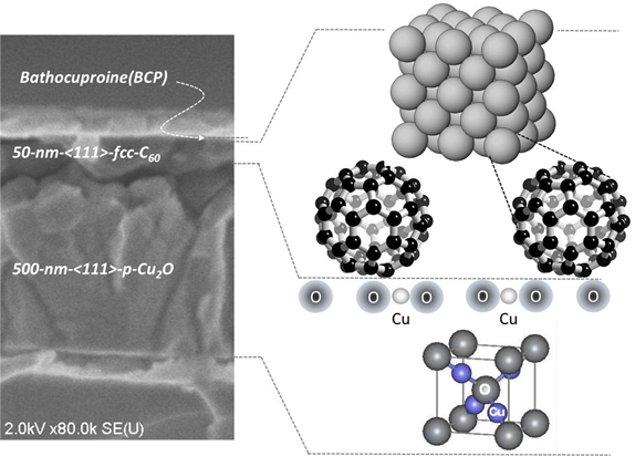
Fig.1:FE-SEM image of the cross-section of the hybrid p-Cu2O/C60/BCP photovoltaic device and schematic illustrations of Cu2O and C60 structures.
Enlarge Image

Masanobu Izaki
Enlarge Image