Research highlights
High photosensitivity few-layered MoSe2 back-gated field-effect phototransistors
Two-dimensional (2D) layered materials are now attracting a lot of interest due to their unique optoelectronic properties at atomic thicknesses. Among them, graphene has been mostly investigated, but the zero-gap nature of graphene limits its practical applications. Therefore, 2D layered materials with intrinsic band gaps such as MoS2, MoSe2, and MoTe2 are of interest as promising candidates for ultrathin and high-performance optoelectronic devices.
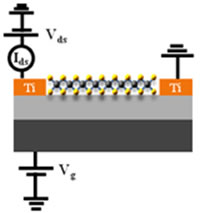
Here, Pil Ju Ko and colleagues at Toyohashi University of Technology, Japan have fabricated back-gated field-effect phototransistors made of MoSe2 crystals having a thickness of only twenty nanometers. The devices were fabricated by mechanical cleavage of MoSe2 crystals into few-layered flakes, followed by transfer onto a silicon wafer with pre-deposited titanium electrodes.
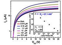
Despite their ultra-thin physical size, the devices showed excellent field-effect phototransistor characteristics. The measured photoresponsivity of 97.1 AW-1 at zero back gate voltage was higher than previous reports of photodetectors fabricated using GaS, GaSe, MoS2, and InSe. The photoresponse of the MoSe2 was much faster (less than 15 msec) than ultrasensitive photodetectors based on monolayer MoS2. Furthermore, the theoretical external quantum efficiency was 280-fold higher than of commercial Si and InGaAs photodiodes.
The research shows that MoSe2 is a promising material for photodetector applications. The group is optimization the device performance by studying thickness-dependent of the photosensitivity.
- Reference:
- Authors: Abdelkader Abderrahmane, Pil Ju Ko, Tran Viet Thu, Shunji Ishizawa, Tsukasa Takamura and Adarsh Sandhu.
- Title of original paper: High photosensitivity few-layered MoSe2 back-gated field-effect phototransistors.
- Journal, volume, pages and year: Nanotechnology 25 365202 (1-5) (2014).
- Digital Object Identifier (DOI): 10.1088/0957-4484/25/36/365202.
- Affiliations: Electronics-Inspired Interdisciplinary Research Institute (EIIRIS) and Department of Electrical and Electronic Information Engineering, Toyohashi University of Technology, 1-1 Hibarigaoka, Tempaku, Toyohashi, Aichi 441-8580, Japan
- Department website: http://www.sandhu.jp/

Pil Ju Ko

Fig.1: Schematic structure of the few-layered MoSe2 FETs.
Enlarge Image

Fig.2:Laser power dependence of the drain current versus the drain-source voltage at zero gate voltage. Inset: photoresponsivity extracted from the Id-Vds characteristic.
Enlarge Image


