
ここからコンテンツです。
New bimetallic alloy nanoparticles for printed electronic circuits
Production of oxidation-resistant copper alloy nanoparticles by electrical explosion of wire for printed electronics By Go Kawamura
Go Kawamura, in cooperation with researchers at Duke University, has invented a production method for oxidation-resistant copper alloy nanoparticles for printed electronics. These novel nanoparticles were produced by an environmentally friendly and economical “wire explosion” method. This invention will expand the application range of printed electronics.
“Printed electronics” has the potential to enable low-cost fabrication of electronics on flexible or curved surfaces, which will lead to the use of electronics in more varied applications. We will be able to fabricate homemade mobile phones or smart watches using a printer in the future. However, the low performance and high cost of current conductive inks have been limiting the advancement of printed electronics.
Now, Go Kawamura and his collaborators at Duke University have found a way to produce new copper alloy nanoparticles, which can be used as the main component of affordable conductive inks with high oxidation resistance. The researchers electrically exploded alloy or twisted metal wires in water with a mild reducing agent (Vitamin C) in order to produce the nanoparticles. The reduction in conductivity was subsequently measured under harsh conditions (high temperature and high humidity).
"We had been working on developing a ‘wire explosion’ method to produce novel metal nanoparticles. Then, we found that some of the produced copper alloy nanoparticles possessed both high oxidation resistance and low electrical resistance," explains Assistant Professor Go Kawamura. "Moreover, the nanoparticles have the advantage of being inexpensive because the production process is very economical and environmentally friendly."
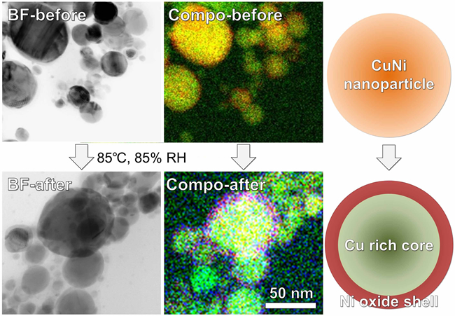
As a result, copper nanoparticles alloyed with 1% Sn, 5% Ag, 5% Ni, or 30% Ni had electrical conductivities similar to that of copper; however, unlike copper, the nanoparticles remained conductive after 24 h at 85 °C and 85% relative humidity. With further improvement of the electrical conductivity and oxidation resistance, copper alloy nanoparticles prepared by wire explosion could be used for the production of high-performance affordable conductive inks, which will contribute to the advancement of printed electronics. The researchers also hope this work will encourage further study combining wire explosion with chemical modification of the explosion medium to control the composition and surface chemistry of nanoparticles.
Reference
Go Kawamura, Samuel Alvarez, Ian E. Stewart, Matthew Catenacci, Zuofeng Chen & Yoon-Cheol Ha (2015). Production of oxidation-resistant Cu-based nanoparticles by wire explosion, Scientific Reports, 5:18333, 1-8. 10.1038/srep18333
プリンテッドエレクトロニクス用の新しい合金ナノ粒子
ワイヤーエクスプロージョン法による高酸化耐性銅合金ナノ粒子の作製とプリンテッドエレクトロニクスへの応用河村剛助教は、米国Duke大学との共同研究を行い、プリンテッドエレクトロニクス用の高酸化耐性銅合金ナノ粒子の新しい合成法を開発した。得られる新規ナノ粒子は、環境負荷が小さく、安価な手法で生産される。この発見により、プリンテッドエレクトロニクスの応用範囲が大きく広がることが期待される。
“プリンテッドエレクトロニクス”はフレキシブル基盤上に安価に電子装置を製作できるため、電子装置の応用範囲を大きく広げる技術として期待されている。しかし、現在の導電インクの低性能と高価格のために、プリンテッドエレクトロニクスは広い応用に至っていない。
河村剛助教と米国Duke大学の研究者らは、安価で高い酸化耐性を有する導電インクの主原料となりうる新規銅合金ナノ粒子の合成方法を新たに開発した。研究者らは、弱い還元剤(ビタミンC)を含む水中で、電気的に金属細線を爆発させてナノ粒子を得た。その粒子を用いて作製した導電ラインの導電性劣化過程は、厳しい環境下(高温、高湿度下)において測定された。
「我々は“ワイヤーエクスプロージョン法”を用いた新規金属ナノ粒子の合成に関して研究を行ってきました。その中で、得られたいくつかの新規銅合金ナノ粒子が高い酸化耐性と低い電気抵抗率を示すことを発見しました。」と河村剛助教は話す。「さらに、低環境負荷で低コストな手法で合成されるこれらのナノ粒子は、きわめて安価に供給できるメリットを有します。」
結果として、1%の錫、5%の銀、5または30%のニッケルと合金化された銅ナノ粒子は、銅単体のナノ粒子と同等の導電率を有しながら、85°C、85%相対湿度の厳しい環境下においても、24時間後に高い導電率を維持していた。さらなる導電率と酸化耐性の向上が達成されれば、ワイヤーエクスプロージョン法で合成される銅合金ナノ粒子が、安価で高性能な導電インクの作製に利用され、プリンテッドエレクトロニクスの広い応用に繋がると期待される。研究者らは、今回のワイヤーエクスプロージョン法と液相化学反応を組み合わせた新しいナノ粒子合成法が、組成や表面化学状態の制御された新規ナノ粒子の合成を目指す研究にも寄与できると期待している。
Researcher Profile

| Name | Go Kawamura |
|---|---|
| Affiliation | Department of Electrical and Electronic Information Engineering |
| Title | Assistant Professor |
| Fields of Research | Nanomaterials Science |
ここでコンテンツ終わりです。